Light emitter with metal-oxide coating

a technology of metal oxide coating and light emitter, which is applied in the direction of basic electric elements, electrical equipment, semiconductor devices, etc., can solve the problems of limited efficiency of leds, increased chance of reabsorption and loss, and significant absorption loss of conventional leds, so as to enhance the light output

Inactive Publication Date: 2013-09-05
KK TOSHIBA
View PDF2 Cites 38 Cited by
  • Summary
  • Abstract
  • Description
  • Claims
  • Application Information

AI Technical Summary

Benefits of technology

[0007]This invention relates generally to light emitting devices and more particularly to new combinations for enhancing their light output.
[0008]One object of the present invention is to provide a low cost device structure with improved light extraction efficiency. In contrast to the prior art no changes are made in the basic semiconductor portion of a light emitting device, so that virtually all of current light emitting diodes or other light emitting device structures can employ the benefits of this invention. The invention improves light extraction from LEDs by providing a medium, as a coating material, that light can enter easily and can propagate through with minimum attenuation. Surfaces of the medium may be configured to facilitate light exiting into air or an encapsulant. Additionally, the invention improves light extraction by greatly increasing the surface area of the device.

Problems solved by technology

However, the efficiency of LEDs is limited by their inability to couple all of the light that is generated by an active layer out of the LED chip.
This light is repeatedly reflected, greatly increasing its chance for reabsorption and loss.
While reflective contacts improve light extraction, conventional LEDs still suffer from significant absorption losses.
Also, roughened surfaces can cause other problems with the LED fabrication process.
For example, contacts to roughened surfaces can be problematic.
Also, roughened surfaces can cause it to be difficult to align photomasks to the wafer.
And they make it difficult for the pattern recognition equipment that are used to bond and inspect the wafers to work properly.
This technique is effective at improving light extraction; however, the textured surface of the substrate affects the subsequent growth of the semiconductor layers.
The quality of the semiconductor layers is often adversely affected, and the reproducibility of the growth is poor.
All of the prior art suffer from marginal improvement of light extraction efficiency or high manufacturing cost or both.

Method used


Image

  • Light emitter with metal-oxide coating
  • Light emitter with metal-oxide coating
  • Light emitter with metal-oxide coating

Examples


Embodiment Construction

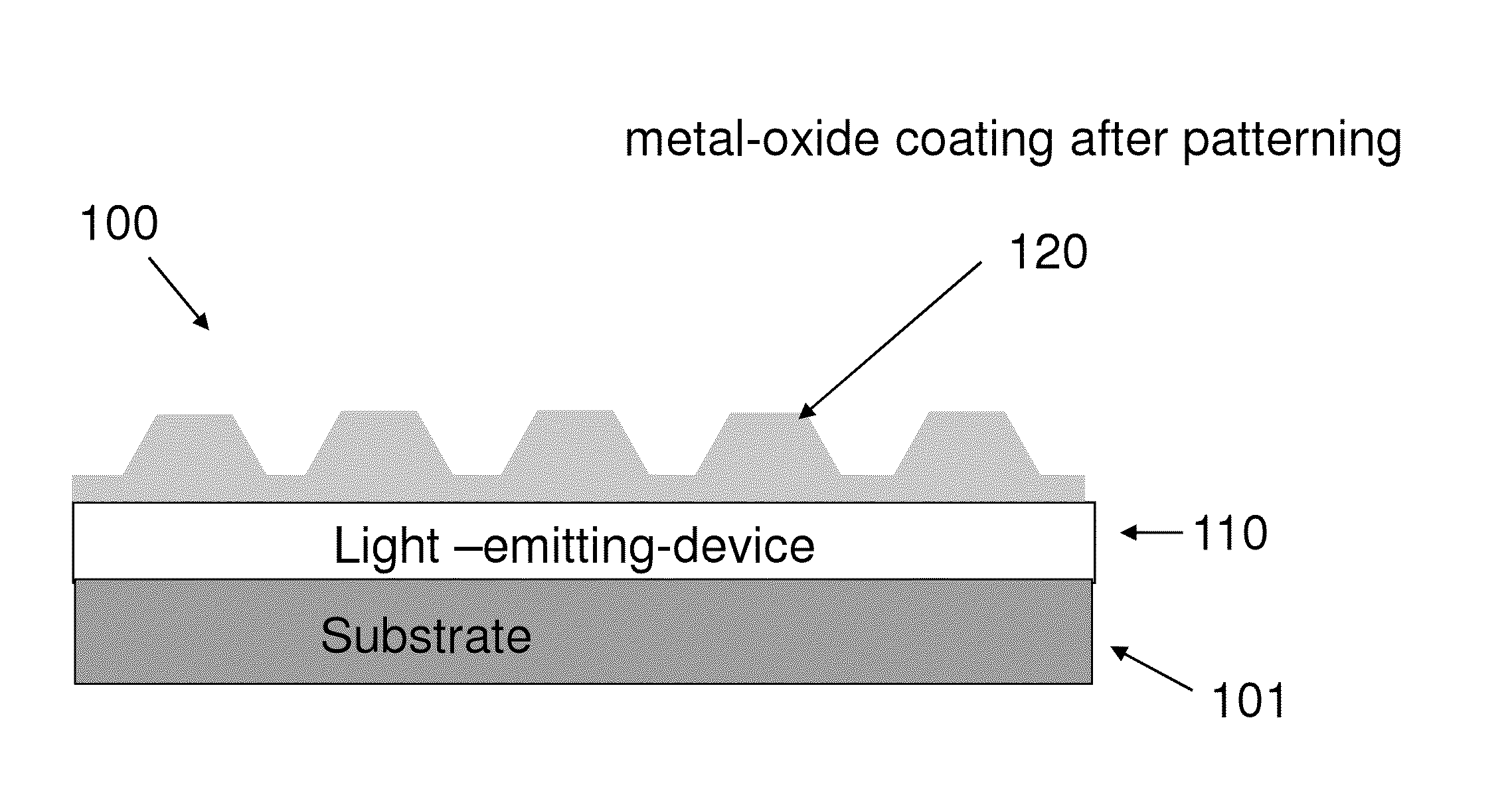
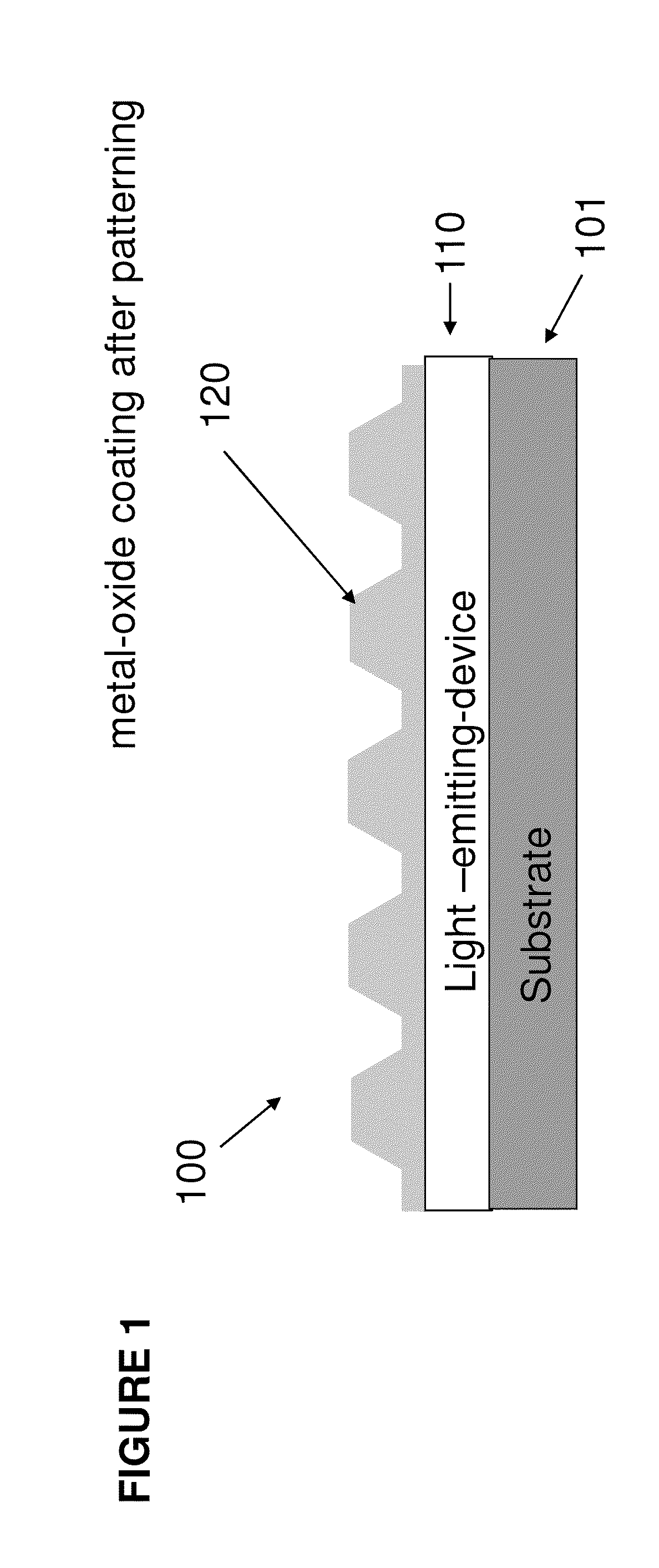
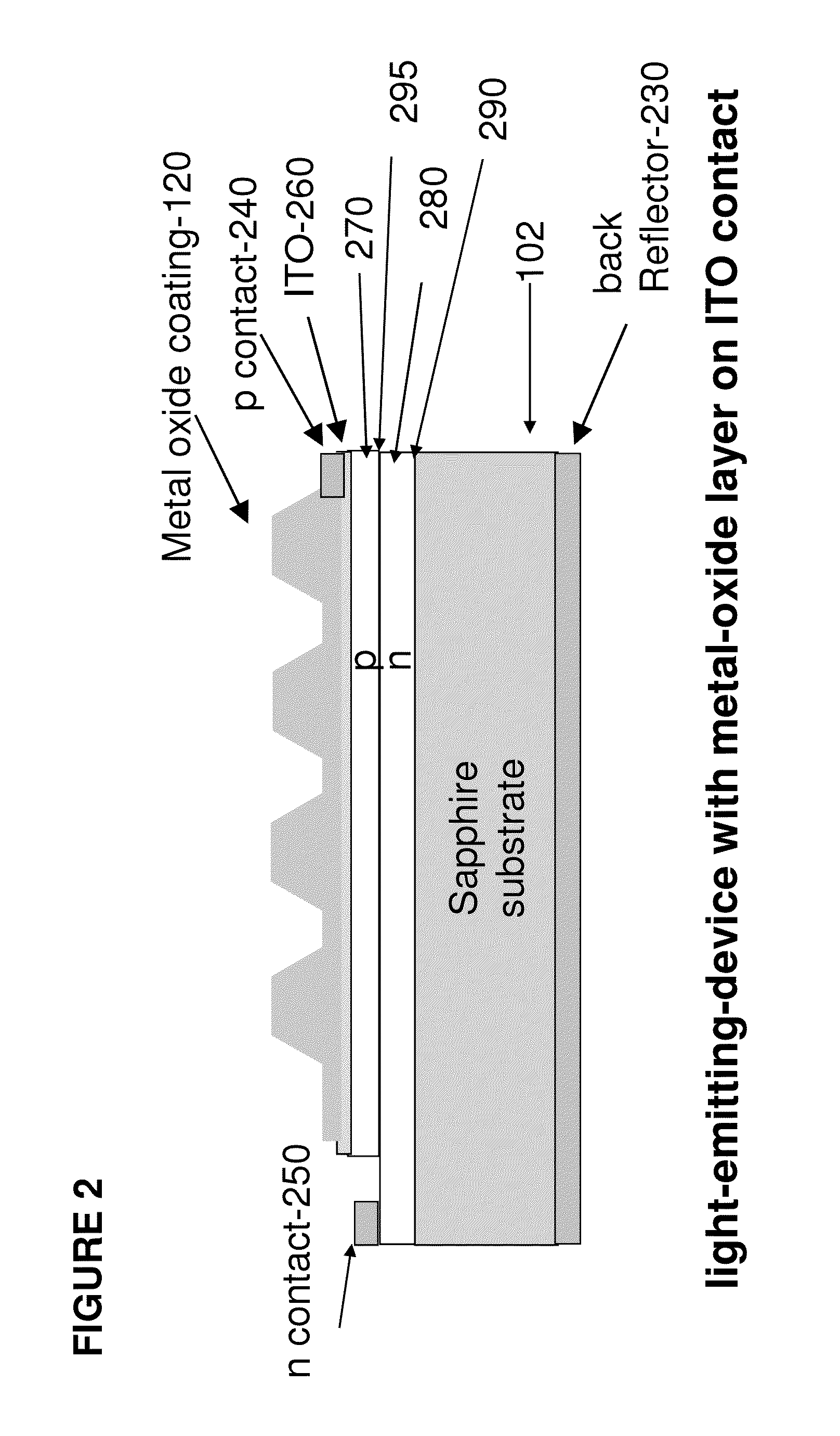
[0020]FIG. 1 shows a schematic view of one embodiment of the invented light emitting structure 100 comprising a substrate portion 101, a light emitting device portion 110 and a metal-oxide coating portion 120. As used herein a substrate or submount portion provides at least a mechanical support for a light emitting device portion and metal-oxide coating portion. A substrate is chosen from a group comprising Al2O3, Si, SiC, AlInGaN based materials, metals, ceramics and glasses; these materials may be single crystal or not. A submount is chosen based on manufacturing convenience; typically a submount is chosen from a group comprising Al2O3, Si, SiC, metals, ceramics, plastics and glasses. As used herein a light emitting device portion is chosen from a group comprising light emitting diodes, light emitting heterojunctions, light emitting quantum well structures and other solid state devices capable of emitting light. As used herein a metal-oxide coating portion is chosen from a group c...


PUM

PropertyMeasurementUnit
thicknessaaaaaaaaaa
thicknessaaaaaaaaaa
index of refractionaaaaaaaaaa

Abstract

A light emitting device based on a AlInGaN materials system wherein a coating is used to improve the extraction of light from a device. A coating has a very low optical loss and an index of refraction greater than 2. In a preferred embodiment the coating is made from Ta2O5, Nb2O5, TiO2, or SiC and has a thickness between about 0.01 and 10 microns. A surface of a coating material may be textured or shaped to increase its surface area and improve light extraction. A surface of the coating material can also be shaped to engineer the directionality of light escaping the layer. A coating can be applied directly to a surface or multiple surfaces of a light emitting device or can be applied onto a contact material. A coating may also serve as a passivation or protection layer for a device.

Description

BACKGROUND OF THE INVENTION[0001]Light emitting devices (LEDs) are an important class of solid state devices that convert electric energy to light and commonly comprise an active layer of semiconductor material sandwiched between additional layers. As the quality of semiconductor materials have improved, the efficiency of LEDs has also improved. Commercially-available LEDs are being made from alloys of indium, aluminum, and gallium with nitrogen (AlInGaN). These alloys make possible LEDs which operate in the ultra-violet to green spectral regions. However, the efficiency of LEDs is limited by their inability to couple all of the light that is generated by an active layer out of the LED chip. When an LED is energized, light emitting from its active layer (in all directions) reaches the LED surfaces at many different angles. Typical semiconductor materials have a high index of refraction compared to ambient air (n=1.0) or encapsulating epoxy (n≈1.5). According to Snell's law, light tr...

Claims


Application Information

Patent Timeline
Patent Type & Authority Applications(United States)
IPC IPC(8): H01L33/44
CPCH01L33/44H01L33/32H01L33/46
Inventor LESTER, STEVEN D.
Owner KK TOSHIBA
Why Eureka
Try Eureka