Gallium nitride based compound semiconductor light-emitting element and method for fabricating the same

a technology of compound semiconductors and light-emitting elements, which is applied in semiconductor/solid-state device manufacturing, semiconductor devices, electrical equipment, etc., can solve the problems of reducing the luminous efficiency and the recombination of carriers in the light-emitting layer, and achieve good electric characteristics, reliability and electric characteristics. good

Inactive Publication Date: 2013-09-12
PANASONIC INTELLECTUAL PROPERTY MANAGEMENT CO LTD
View PDF3 Cites 11 Cited by
  • Summary
  • Abstract
  • Description
  • Claims
  • Application Information

AI Technical Summary

Benefits of technology

[0017]According to the above aspect, diffusion of hydrogen from a p-type layer into an active layer, which will ordinarily often occur in an m-plane semiconductor multilayer structure, can be reduced. In addition, the p

Problems solved by technology

As a result, the probability of radiative recombination of carriers in the li

Method used


Image

  • Gallium nitride based compound semiconductor light-emitting element and method for fabricating the same
  • Gallium nitride based compound semiconductor light-emitting element and method for fabricating the same
  • Gallium nitride based compound semiconductor light-emitting element and method for fabricating the same

Examples


embodiment

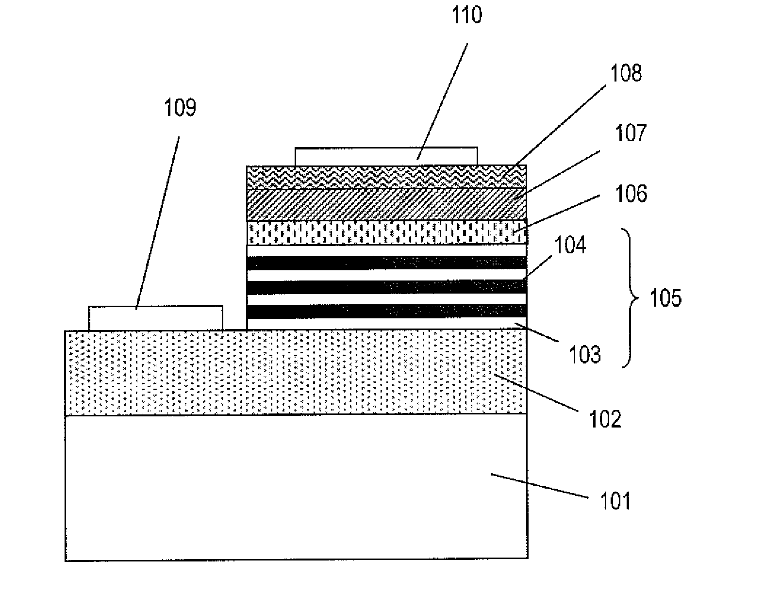
[0107]Hereinafter, an embodiment of a gallium nitride based compound semiconductor light-emitting element and method for fabricating such an element according to the present disclosure will be described with reference to FIG. 12.

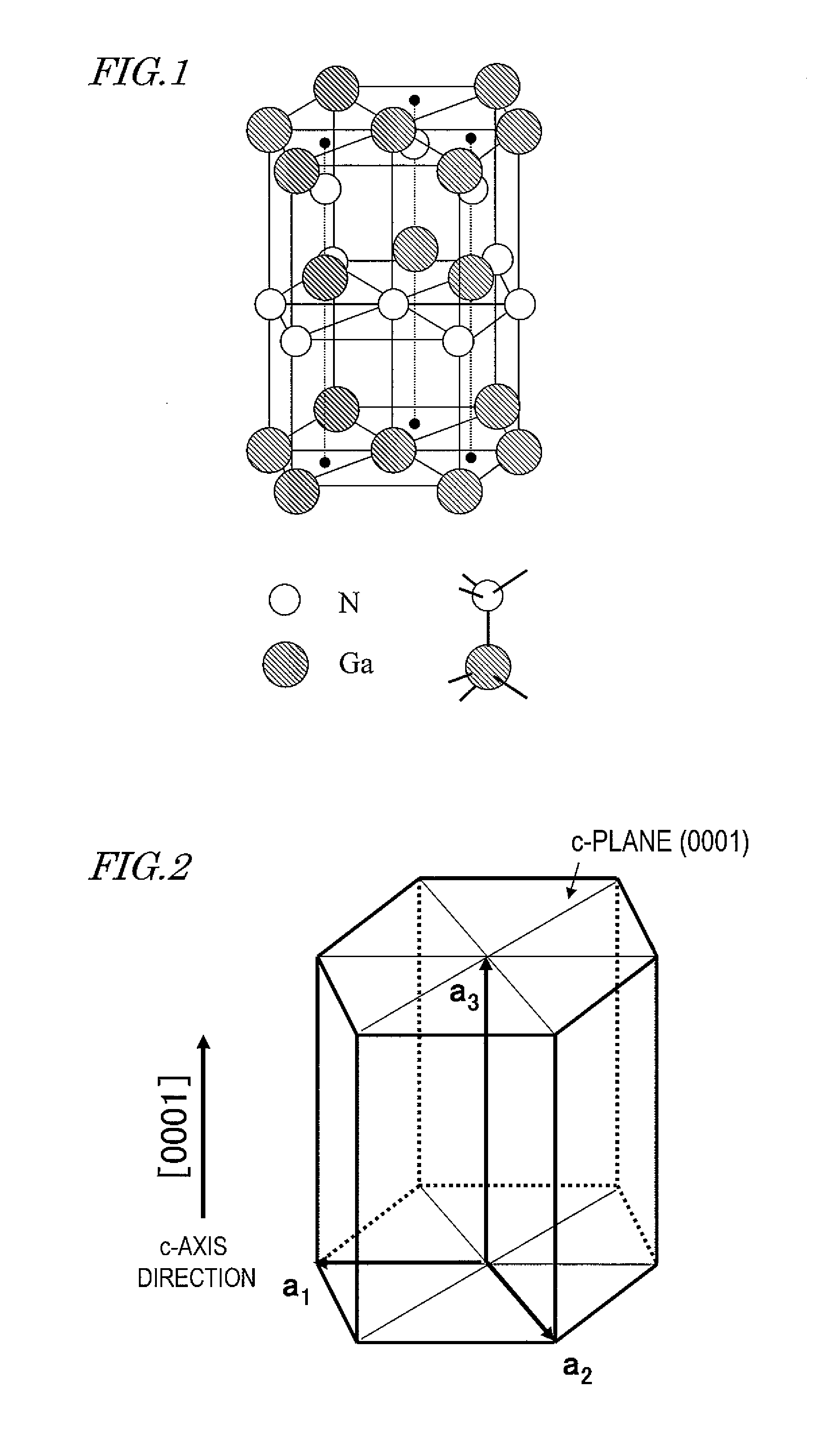
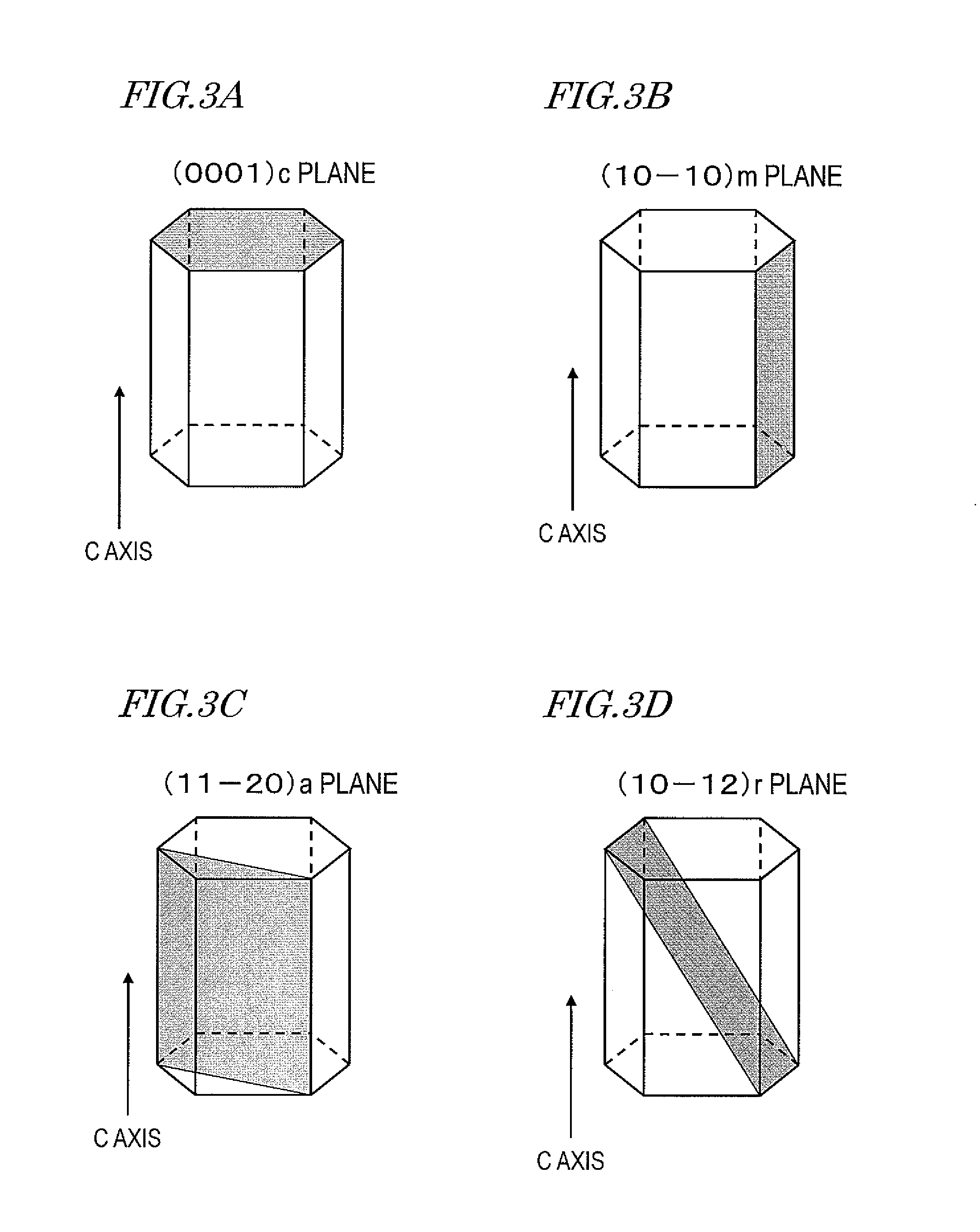
[0108]The gallium nitride based compound semiconductor light-emitting element of this embodiment includes an n-type gallium nitride based compound semiconductor layer 102, a p-type gallium nitride based compound semiconductor layer 107, and an active layer 105 which is arranged between the n- and p-type gallium nitride based compound semiconductor layers 102 and 107. The active layer 105 and the p-type gallium nitride based compound semiconductor layer 107 are m-plane semiconductor layers. The p-type gallium nitride based compound semiconductor layer 107 includes magnesium at a concentration of 2.0×1018 cm−3 to 2.5×1019 cm−3 and oxygen, of which the concentration is 5% to 15% of the concentration of the magnesium. Alternatively, the p-type gallium nitride ba...


PUM


Abstract

A gallium nitride based compound semiconductor light-emitting element according to an embodiment of the present disclosure includes: an n-type gallium nitride based compound semiconductor layer; a p-type gallium nitride based compound semiconductor layer; and an active layer which is arranged between the n- and p-type gallium nitride based compound semiconductor layers. The active layer and the p-type gallium nitride based compound semiconductor layer are m-plane semiconductor layers. The p-type gallium nitride based compound semiconductor layer includes magnesium at a concentration of 2.0×1018 cm−3 to 2.5×1019 cm−3 and oxygen, of which the concentration is 5% to 15% of the concentration of the magnesium.

Description

[0001]This is a continuation of International Application No. PCT / JP2012 / 002291, with an international filing date of Apr. 2, 2012, which claims priority of Japanese Patent Application No. 2011-087949, filed on Apr. 12, 2011, the contents of which are hereby incorporated by reference.BACKGROUND[0002]1. Technical Field[0003]The present application relates to a gallium nitride based compound semiconductor light-emitting element and a method for fabricating such an element.[0004]2. Description of the Related Art[0005]A nitride semiconductor including nitrogen (N) as a Group V element is a prime candidate for a material to make a short-wave light-emitting element, because its bandgap is sufficiently wide. Among other things, gallium nitride-based compound semiconductors (which will be referred to herein as “GaN-based semiconductors”) have been researched and developed particularly extensively. As a result, blue-ray-emitting light-emitting diodes (LEDs), green-ray-emitting LEDs and semic...

Claims


Application Information

Patent Timeline
IPC IPC(8): H01L33/14H01L33/06
CPCH01L33/007H01L33/025H01L33/16H01L33/145H01L33/14H01L33/06H01L33/32
Inventor KATO, RYOUYOSHIDA, SHUNJICHOE, SONGBAEKYOKOGAWA, TOSHIYA
Owner PANASONIC INTELLECTUAL PROPERTY MANAGEMENT CO LTD
Why Eureka
Try Eureka