Thin film forming method

a film formation and thin film technology, applied in the direction of vacuum evaporation coating, superimposed coating process, semiconductor/solid-state device details, etc., can solve the problem of insufficient improvement of electromigration resistance, improve electromigration resistance, improve adhesion

Inactive Publication Date: 2013-09-26
TOKYO ELECTRON LTD
View PDF4 Cites 13 Cited by
  • Summary
  • Abstract
  • Description
  • Claims
  • Application Information

AI Technical Summary

Benefits of technology

[0010]In view of the above, the present invention provides a thin film forming method capable of improving adhesivity with a metal to be filled and filling characteristics and improving an electromigration resistance.
[0011]As a result of examination, the present inventors have conceived the present invention by discovering that when an annealing process is performed in a state where a metal film having a lattice spacing that is close to that of a material of a metal layer for filling is formed on a top surface of the metal layer for filling, grains in the metal layer for filling is effectively grown and, thus, an electromigration resistance can be improved.
[0012]In accordance with the present invention, there is provided a thin film forming method in which a thin film is formed on a surface of a target object to be processed to fill a recess formed in the surface of the target object, the method includes the steps of forming a metal layer for filling on the surface of the target object to fill the recess formed in the surface of the target object; forming a metal film for preventing diffusion on an entire surface of the target object to cover the metal layer for filling; and annealing the target object having the metal film for preventing diffusion formed thereon.

Problems solved by technology

However, the film formation method described in JP2004-335998A is disadvantageous in that a grain size of a crystal grain of the copper film is comparatively small and electromigration resistance cannot be improved sufficiently in spite of the annealing process.
However, the purpose of JP2006-303062A is not to improve an electromigration resistance but to move crystal defects in the conductive film to the interface between the conductive film and the coating film and improve the crystal defects.

Method used


Image

  • Thin film forming method
  • Thin film forming method
  • Thin film forming method

Examples


Embodiment Construction

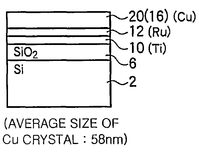
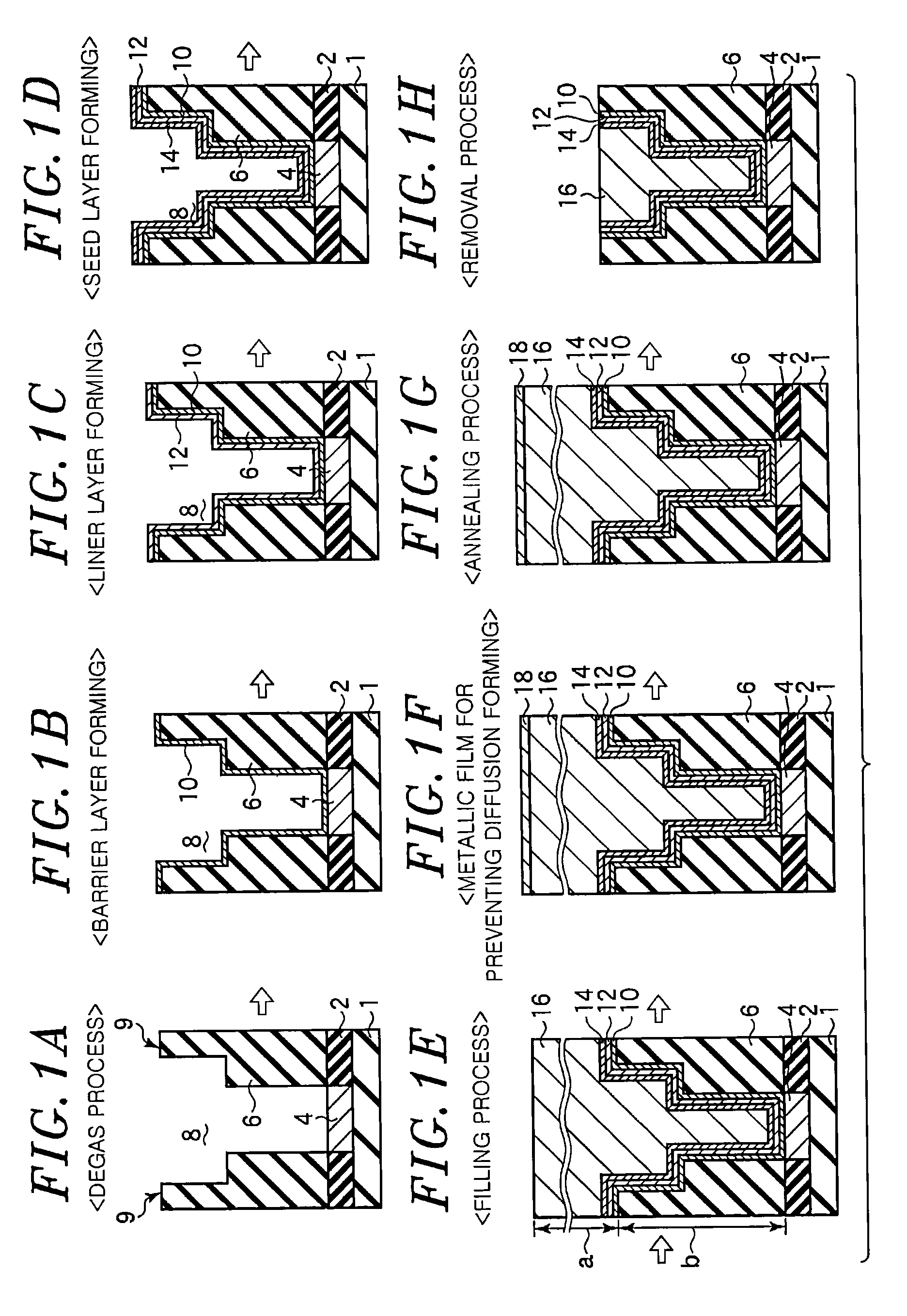
[0025]Hereinafter, an embodiment of the present invention will be described in detail with reference to the accompanying drawings which form a part hereof. Here, the case in which copper (Cu) is used for a metal layer for filling and ruthenium (Ru) is used for a liner layer will be described as an example.

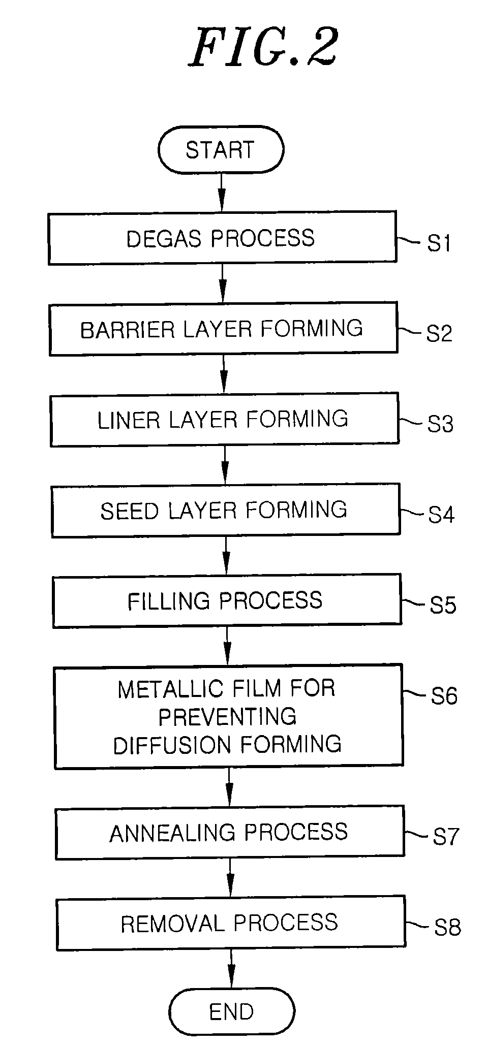
[0026]FIGS. 1A to 1H are cross sectional views showing a state of a semiconductor wafer as a target object to be processed in each process of a thin film forming method in accordance with an embodiment of the present invention. FIG. 2 is a flowchart showing the thin film forming method in accordance with the embodiment of the present invention.

[0027]Here, insulating layers 1 and 2 are sequentially formed on a surface of a silicon substrate shown in FIG. 1A which serves as a target object to be processed. Next, a conductive layer 4 formed of a wiring layer or the like is formed in the insulating layer 2. Thereafter, an insulating layer 6 formed of, e.g., a SiO2 film or the like, whi...


PUM

PropertyMeasurementUnit
temperatureaaaaaaaaaa
thicknessaaaaaaaaaa
thicknessaaaaaaaaaa

Abstract

A thin film forming method in which a thin film is formed on a surface of a target object to be processed to fill a recess formed in the surface of the target object includes the steps of forming a metal layer for filling on the surface of the target object to fill the recess formed in the surface of the target object and forming a metal film for preventing diffusion on an entire surface of the target object to cover the metal layer for filling. The thin film forming method further includes the step of annealing the target object having the metal film for preventing diffusion formed thereon.

Description

[0001]This application is a Continuation Application of PCT International Application No. PCT / JP2011 / 055674 filed on Mar. 10, 2011, which designated the United States.FIELD OF THE INVENTION[0002]The present invention relates to a thin film formation method used for filling a recess formed in a target object to be processed such as a semiconductor wafer or the like.BACKGROUND OF THE INVENTION[0003]In general, a desired semiconductor device is manufactured by repeatedly performing various processes such as a film forming process, a pattern etching process and the like on a semiconductor wafer. Recently, due to a demand for high integration and high miniaturization of a semiconductor device, a line width or a hole diameter is getting finer. Although an aluminum alloy has been conventionally used as a wiring material or a filling material, tungsten W or copper Cu tends to be recently used in order to meet the demand for miniaturization of a line width or a hole diameter and increase of ...

Claims


Application Information

Patent Timeline
Patent Type & Authority Applications(United States)
IPC IPC(8): H01L21/768
CPCC23C14/025C23C14/18H01L2924/0002C23C14/5806C23C14/5873C23C16/0272C23C16/56H01L21/76846H01L21/76877H01L21/76883H01L23/53238H01L2924/09701H01L21/76829C23C16/08C23C28/322C23C28/345C23C28/42C23C28/34H01L2924/00H01L21/3205
Inventor ISHIZAKA, TADAHIRORULLAN, JONATHANYOKOYAMA, OSAMUGOMI, ATSUSHIYASUMURO, CHIAKIKATO, TAKARAHATANO, TATSUOKAWASAKI, HIROAKI
Owner TOKYO ELECTRON LTD
Why Eureka
Try Eureka