High power high isolation low current CMOS RF switch

a low-current, high-isolation technology, applied in the field of low-current cmos rf switch, can solve the problems of increased competition and price wars, reduced price of components making up the device, and increased actual cost of the components, so as to improve system performance, simplify the implementation of antenna diversity design, and reduce the effect of current consumption

Inactive Publication Date: 2013-09-26
DSP GROUP
View PDF29 Cites 18 Cited by
  • Summary
  • Abstract
  • Description
  • Claims
  • Application Information

AI Technical Summary

Benefits of technology

[0010]Integrating the RF switch in a mixed signal CMOS process simplifies the implementation of an antenna diversity design and therefore improves system performance. The low current consumption of the switch makes it particularly attractive for use in mobile devices. The reduced component count required by the switch is useful when implemented in hand held devices while simplifying application board design and integration and significantly reducing cost.

Problems solved by technology

There are a large number of manufacturers of such devices, which leads to increased competition and price wars.
One of the factors that limit price reduction is the actual cost of the components making up the device, including resistors, capacitors, diodes, etc., which are external to the chip or chip-set that constitute the core of the device.
Placing such components on the device, however, is impossible due to the different technologies used.
For example, PIN diodes cannot be placed on the chip to their unavailability in standard CMOS processes.
The components which are external to the chip or chip-set increase the cost of the device in a number of ways: (1) they must be manufactured or purchased; (2) their assembly within the device incurs resources including equipment and labor; and (3) they consume valuable printed circuit board (PCB) real estate, thus requiring larger printed circuit boards.

Method used


Image

  • High power high isolation low current CMOS RF switch
  • High power high isolation low current CMOS RF switch
  • High power high isolation low current CMOS RF switch

Examples


Embodiment Construction

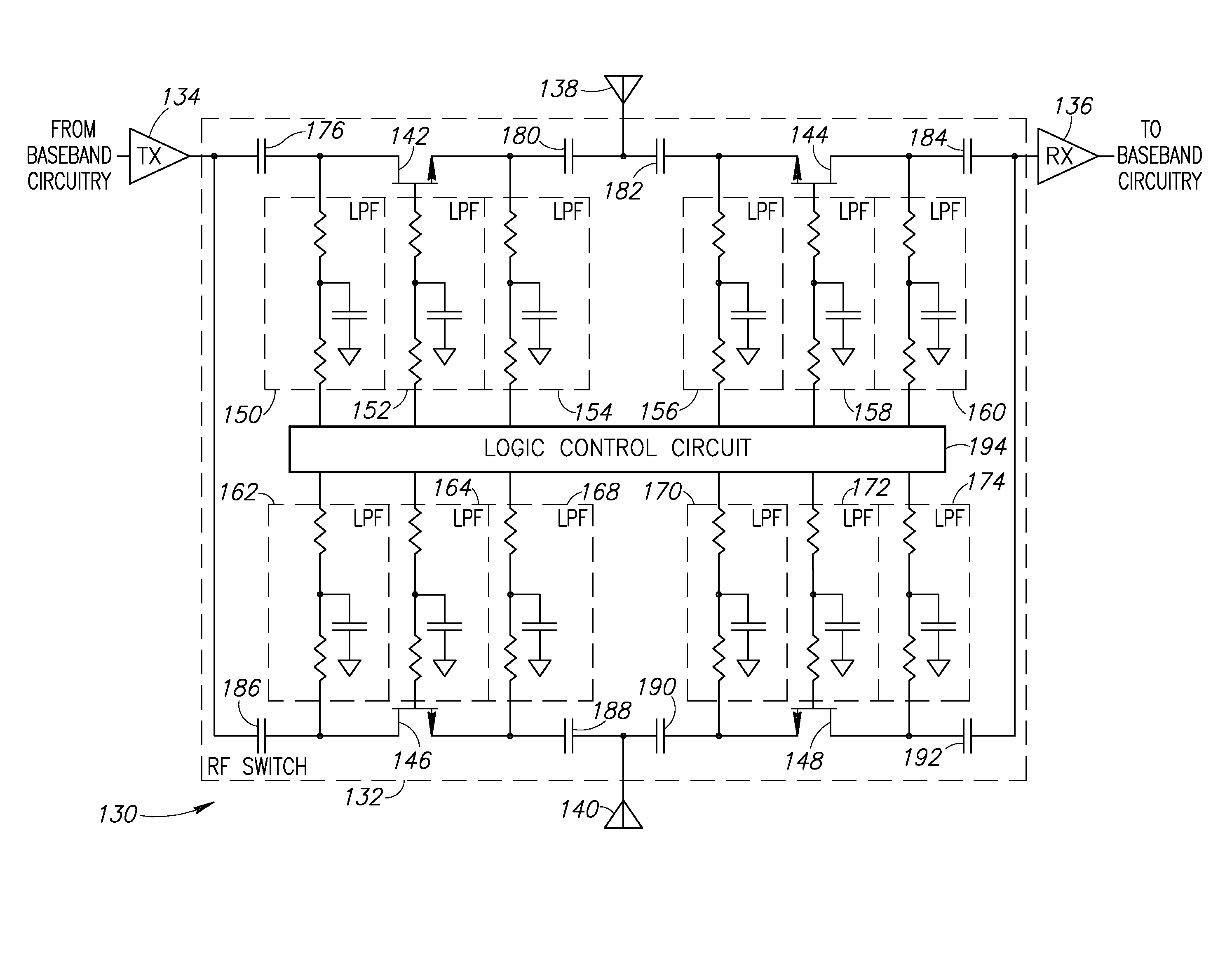
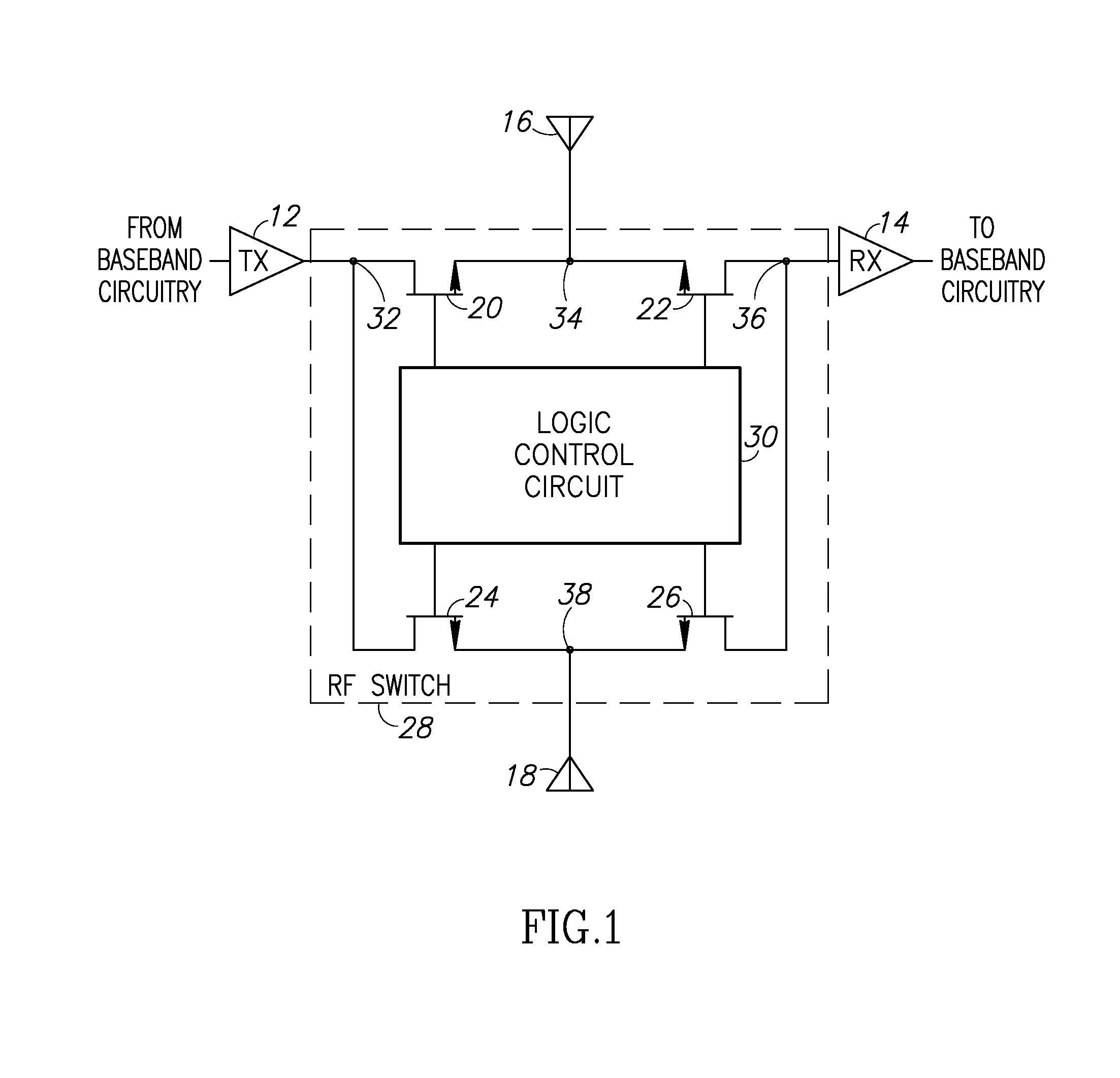
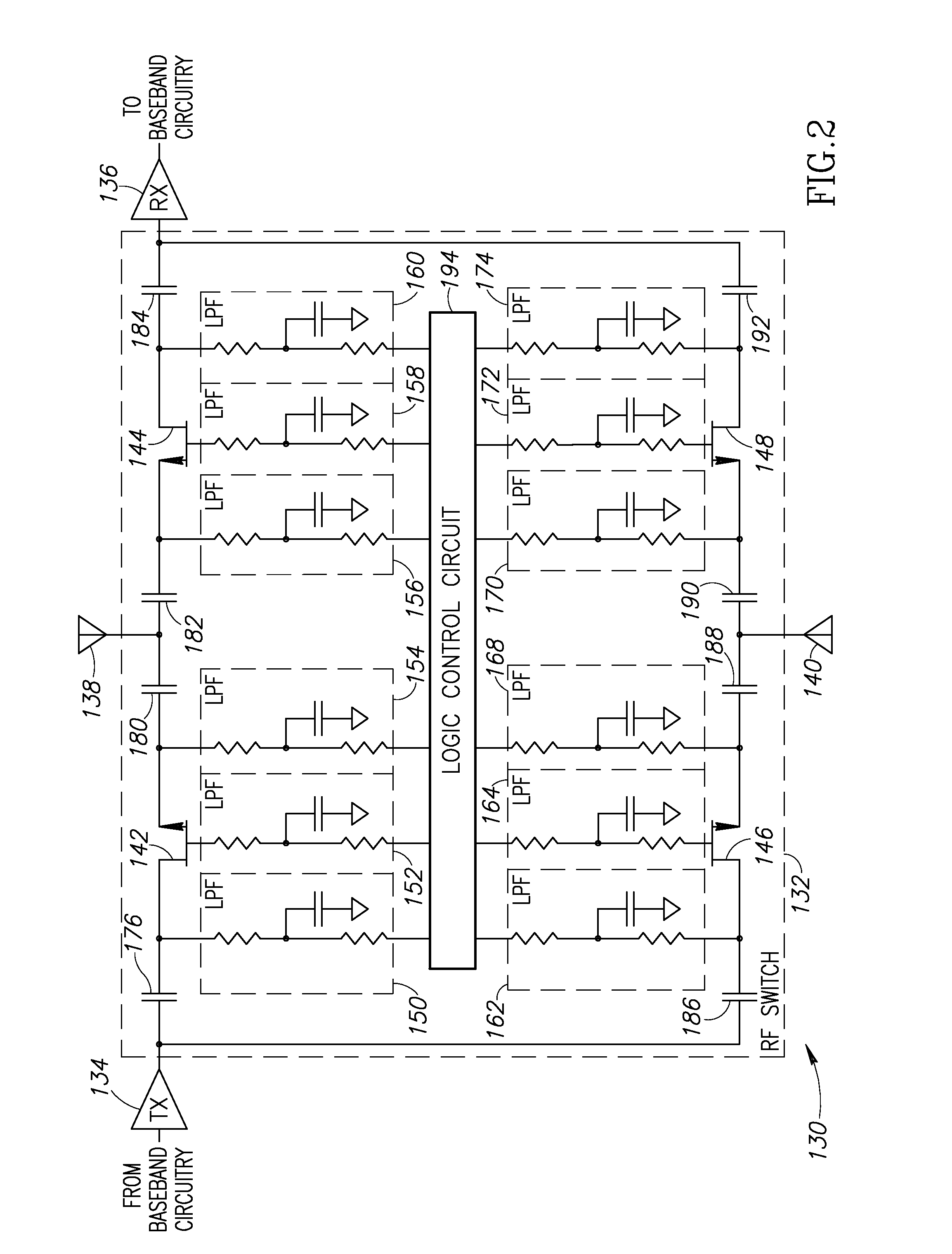
[0020]The transmit / receive (T / R) switch is one of the building blocks typically part of the RF front end circuit of a radio. In addition, an antenna diversity function is known to improve system performance. In one embodiment, a double-pole, double-throw (DPDT) switch is used to couple the transmitter and receiver to either of two antennas.

[0021]In one embodiment, four PIN diodes are used to implement such a DPDT switch along with the appropriate peripheral components that are used for biasing and matching networks. Depending on the technology used for the integrated circuit (IC) transceiver circuitry, the PIN diodes are likely to be external to chip. In addition, to turn PIN diode switch on requires a forward biasing current in the order of 5 to 10 mA. The use of PIN diodes to implement an external DPDT switch, however, increases the bill of materials (BOM), printed circuit board size, board assembly complexity, etc.

[0022]In an alternative embodiment, gallium arsenide (GaAs) based ...


PUM


Abstract

A novel and useful RF switch that comprises four transistors configured to have four operating states, wherein at any time at most one transistor is in ‘on’ state. The switch is an on-chip switch and is constructed in using CMOS processes and technology. The switch is optionally a double pole, double throw (DPDT) switch. The switch can be used in numerous mobile devices such as a cellular phone or in the handset or base station of a cordless phone. The switch optionally selects between two antennas and between transmitter and receiver circuits. Within the switch, at least one of the at least four transistors is optionally an N-channel Metal Oxide Semiconductor (NMOS) transistor. The switch can further comprise one or more logic control circuits providing biasing voltages to one or more of the transistors. Within the switch, the control circuit comprises logic components for providing appropriate biasing voltages to the drain, source and gate terminals of the transistors in the switch.

Description

REFERENCE TO PRIORITY APPLICATION[0001]This application claims priority to and is a continuation in part of U.S. Application Ser. No. 13 / 823,367, filed Mar. 14, 2013, entitled “RF Switch Implementation in CMOS Process,” which is based on PCT / IL2010 / 000787, filed Sep. 21, 2010, entitled “RF Switch Implementation in CMOS Process,” incorporated herein by reference in their entirety.FIELD OF THE INVENTION[0002]The present invention relates to the field of electronic switching, and more particularly relates to a low current CMOS RF switch exhibiting high power capability and high isolation.BACKGROUND OF THE INVENTION[0003]Consumer products such as communication devices and in particular wireless telephones have long become standard commodities. There are a large number of manufacturers of such devices, which leads to increased competition and price wars.[0004]One of the factors that limit price reduction is the actual cost of the components making up the device, including resistors, capa...

Claims


Application Information

Patent Timeline
Patent Type & Authority Applications(United States)
IPC IPC(8): H04B1/44
CPCH04B1/44
Inventor HASSON, YARONMOSTOV, ALEX
Owner DSP GROUP
Why Eureka
Try Eureka