Multilayer ceramic electronic component and fabrication method thereof
a technology of electronic components and ceramics, applied in the direction of fixed capacitors, stacked capacitors, fixed capacitor details, etc., can solve the problems of affecting the reliability of mlcc, difficult to control equivalent series resistance, etc., and achieve the effect of preventing the infiltration of plating solution
- Summary
- Abstract
- Description
- Claims
- Application Information
AI Technical Summary
Benefits of technology
Problems solved by technology
Method used
Image

Examples
first embodiment
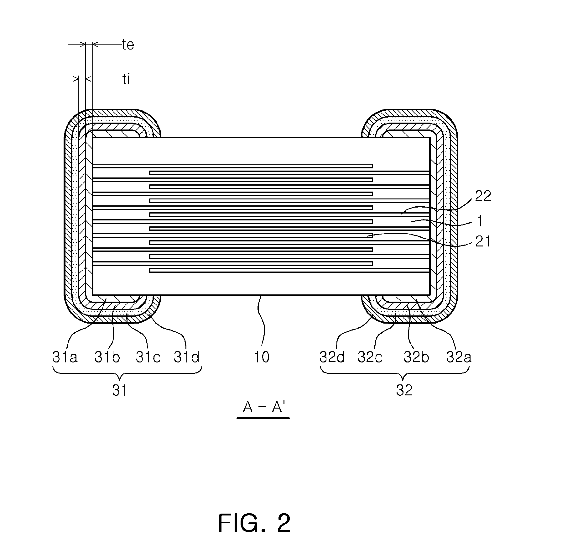
[0035]FIG. 2 is a cross-sectional view of the MLCC, taken along line A-A′ according to the present invention.
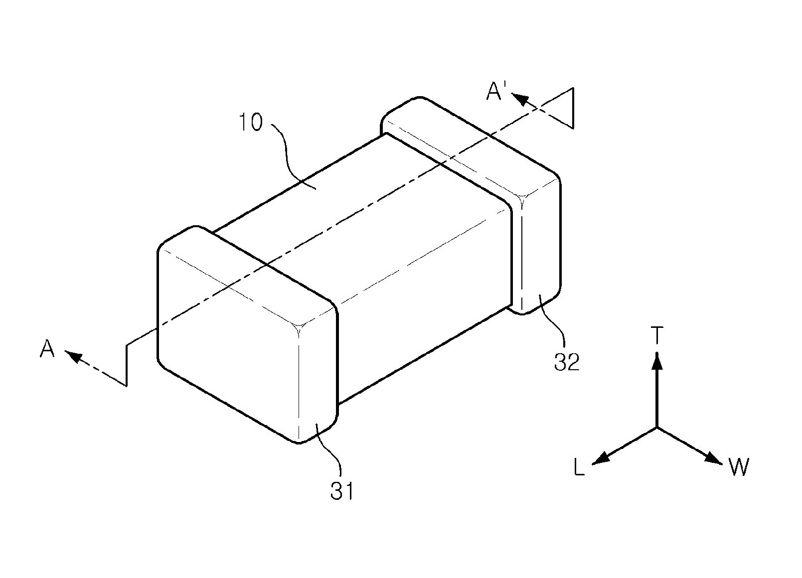
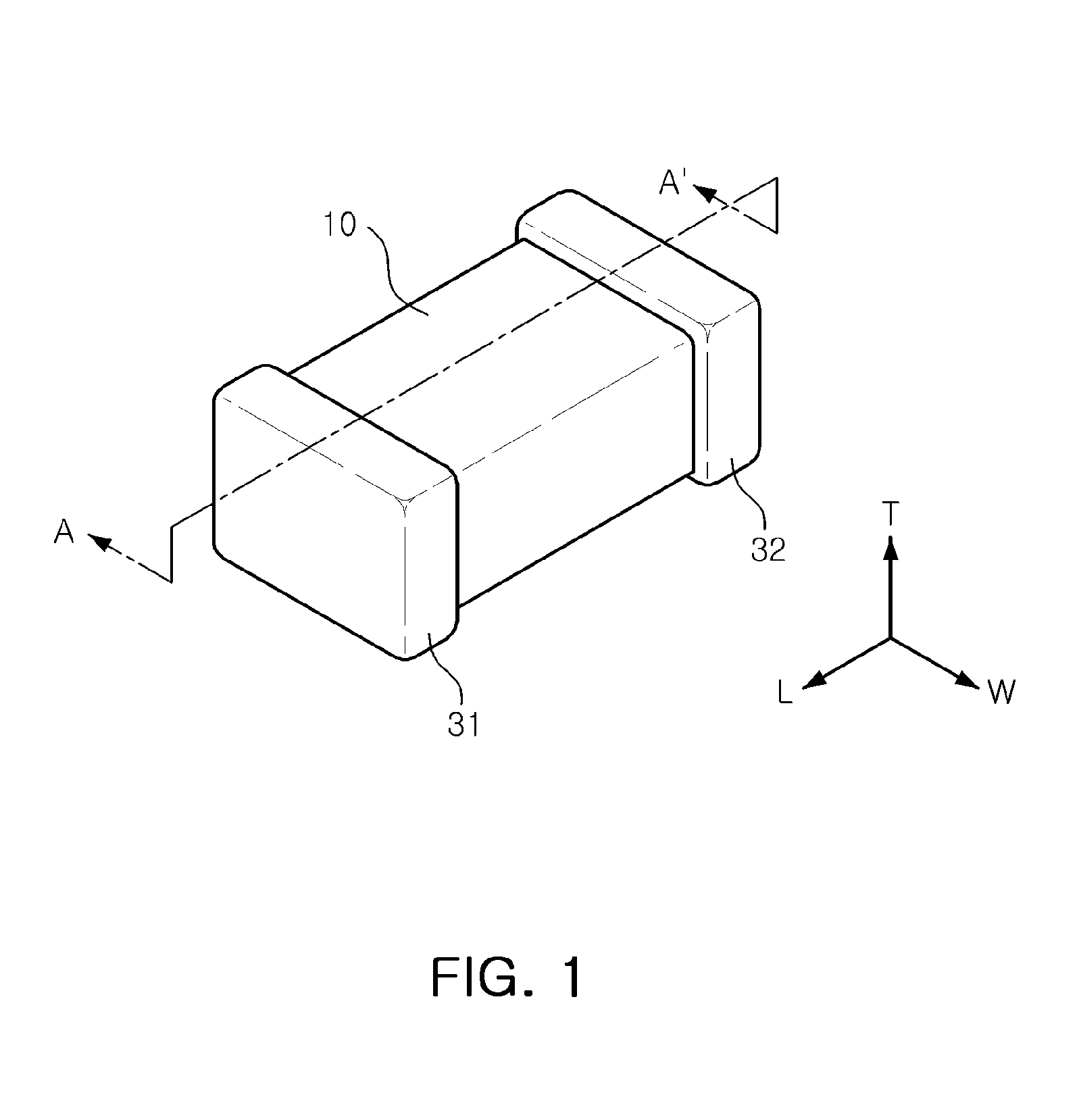
[0036]With reference to FIGS. 1 and 2, the multilayer ceramic electronic component according to the first embodiment of the present invention may include a ceramic main body 10 in which internal electrodes 21 and 22 and dielectric layers 1 are alternately laminated; external electrodes 31a and 32a formed on outer surfaces of the ceramic main body 10; intermediate layers 31b and 32b formed on the external electrodes 31a and 32a and including one or more selected from the group consisting of nickel, copper, and a nickel-copper alloy; and plating layers 31c, 31d, 32c, 32d formed on the intermediate layers.
[0037]Hereinafter, a multilayer ceramic electronic component according to an embodiment of the present invention will be described by using a multilayer ceramic capacitor (MLCC) as an example, but the present invention is not limited thereto.
[0038]In the MLCC according to the e...
second embodiment
[0072]FIG. 3 is a cross-sectional view of the MLCC, taken along line A-A′ according to the present invention.
[0073]With reference to FIG. 3, in the MLCC according to the second embodiment of the present invention, the intermediate layers 31b and 32b may further include copper oxide layers 31b′ and 32b′.
[0074]Namely, in the MLCC according to the second embodiment of the present invention, the intermediate layers 31b and 32b including the copper oxide layers 31b′ and 32b′ and metal layers 31b″ and 32b″ including one or more selected form the group consisting of nickel, copper, and a nickel-copper alloy may be formed on the external electrodes 31a and 32a.
[0075]The intermediate layers 31b and 32b including the copper oxide layers 31b′ and 32b′ and the metal layers 31b″ and 32b″ including one or more selected form the group consisting of nickel, copper, and a nickel-copper alloy, which are sequentially formed, are merely illustrative, and the intermediate layers 31b and 32b may includ...
third embodiment
[0077]FIG. 4 is a flowchart illustrating a process of manufacturing an MLCC according to the present invention.
[0078]With reference to FIG. 4, a method of fabricating a multilayer ceramic electronic component according to the third embodiment of the present invention may include: laminating and sintering ceramic green sheets with internal electrode patterns formed thereon to form a ceramic main body in which dielectric layers and internal electrodes are alternately laminated; forming external electrodes on outer surfaces of the ceramic main body; forming intermediate layers including one or more selected from the group consisting of nickel, copper, and a nickel-copper alloy on the external electrodes; and forming plating layers on the intermediate layers.
[0079]In the method of fabricating the multilayer ceramic electronic component according to the third embodiment of the present invention, first of all, a ceramic green sheet including a dielectric substance may be prepared.
[0080]In...
PUM
| Property | Measurement | Unit |
|---|---|---|
| Temperature | aaaaa | aaaaa |
| Temperature | aaaaa | aaaaa |
| Temperature | aaaaa | aaaaa |
Abstract
Description
Claims
Application Information