Pattern measurement method and pattern measurement apparatus

a measurement method and pattern technology, applied in material analysis using wave/particle radiation, instruments, nuclear engineering, etc., can solve the problem that the above-mentioned method cannot measure such a side wall angl

Inactive Publication Date: 2013-10-10
ADVANTEST CORP +1
View PDF2 Cites 5 Cited by
  • Summary
  • Abstract
  • Description
  • Claims
  • Application Information

AI Technical Summary

Benefits of technology

The present invention provides a pattern measurement method and apparatus capable of measuring a side wall angle of a reverse tapered pattern. This is achieved by acquiring scanning electron microscopic images of the pattern at different acceleration voltages and detecting the change in the white band width of the pattern, which is caused by the side wall angle. The side wall angle can be accurately measured using this method.

Problems solved by technology

As a consequence, the aforementioned method cannot measure such a side wall angle.[Patent Document 1] Japanese Laid-open Patent Publication No. 10-170530[Patent Document 2] Japanese Laid-open Patent Publication No. 2008-71312

Method used


Image

  • Pattern measurement method and pattern measurement apparatus
  • Pattern measurement method and pattern measurement apparatus
  • Pattern measurement method and pattern measurement apparatus

Examples


first embodiment

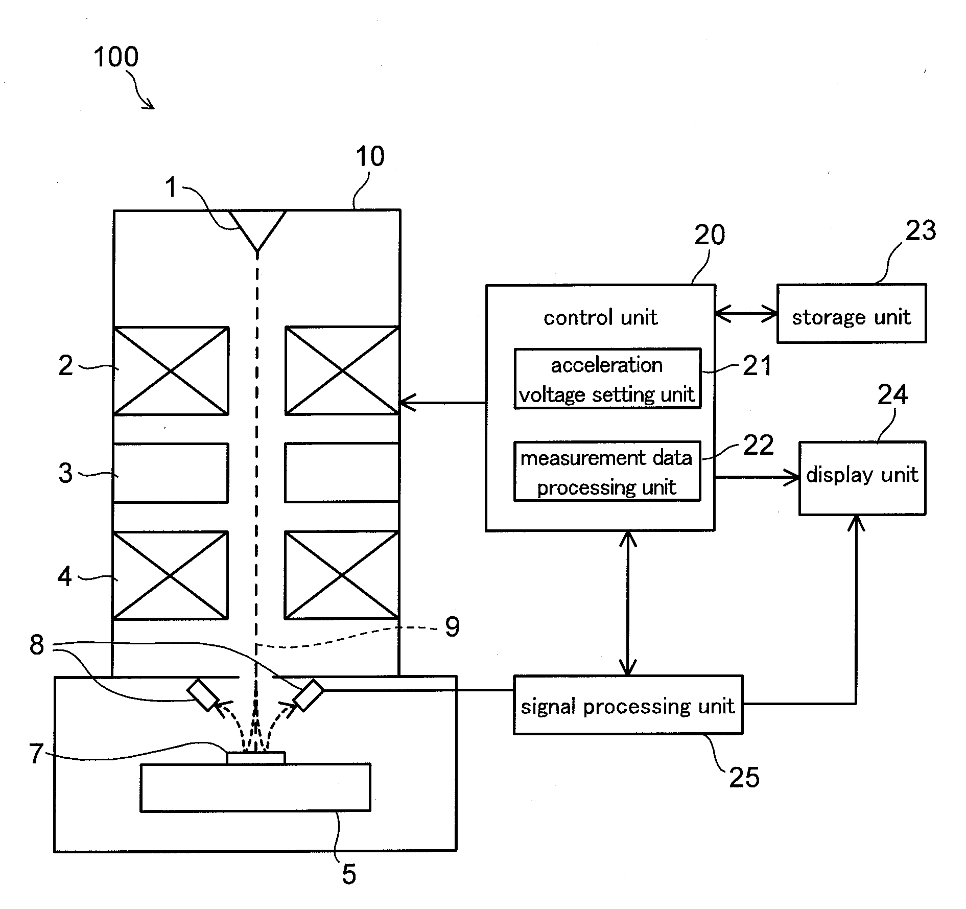
[0020]FIG. 1 is a block diagram of a pattern measurement apparatus according to a first embodiment.

[0021]This pattern measurement apparatus 100 includes an electron scanning unit 10, a control unit 20, a storage unit 23, an image display unit 24, and a signal processing unit 25.

[0022]Among them, the electron scanning unit 10 includes an electron gun 1. The electron gun 1 emits electrons at given acceleration voltages. The electrons emitted from the electron gun 1 are converged with a condenser lens 2 and are thereby converted into an electron beam 9. The electron beam 9 is deflected with a deflection coil 3, then focused with an objective lens 4, and irradiated onto a surface of a sample 7. Thereafter, the electron beam 9 is caused to scan within an observation region on the surface of the sample 7 by using the deflection coil 3.

[0023]Secondary electrons are emitted from the surface of the sample 7 as a consequence of irradiation with the electron beam 9. The emitted secondary elect...

second embodiment

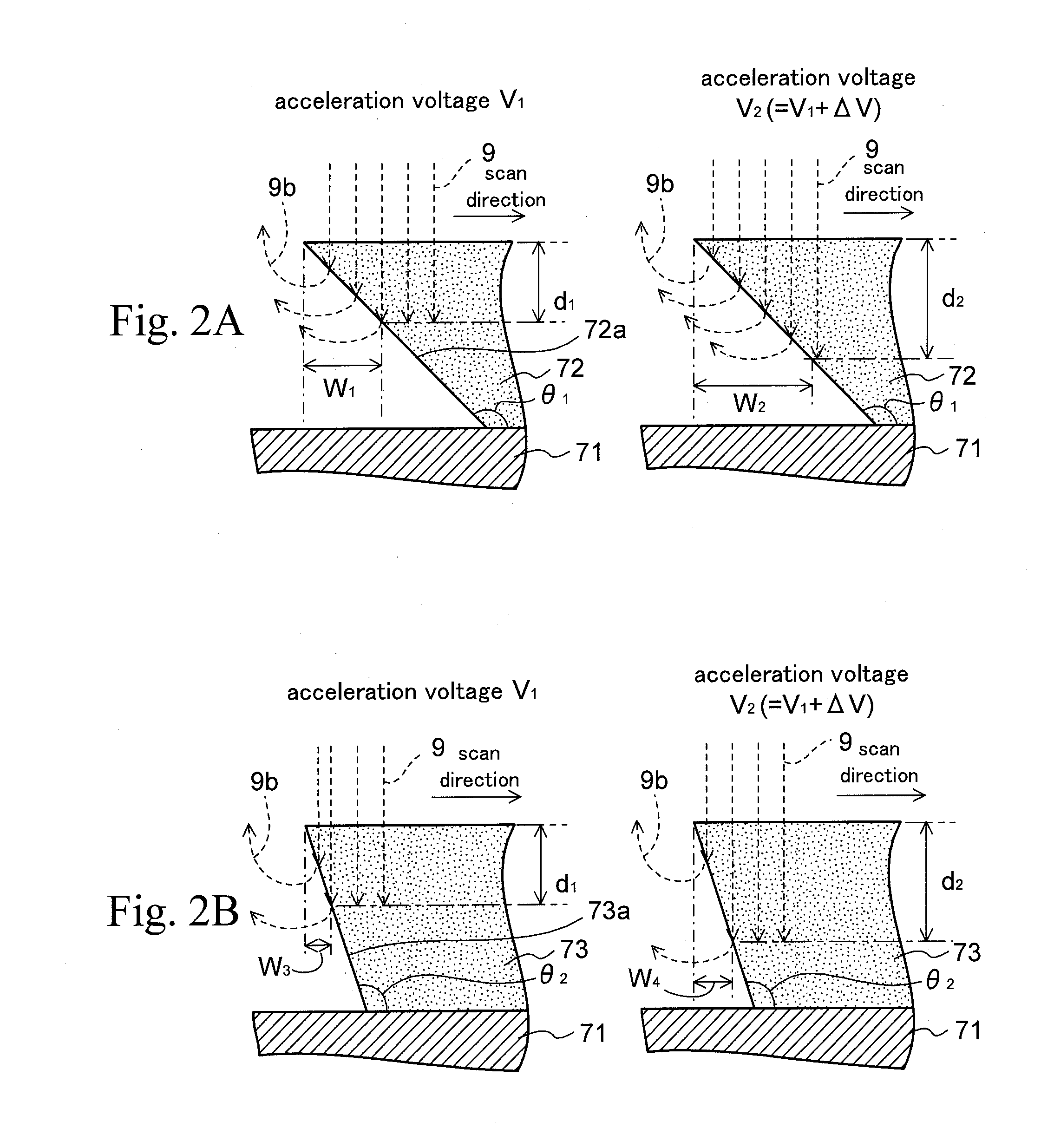
[0072]Researches conducted by the inventors of the present application have found out that a forward tapered pattern having a side wall angle equal to or below 90° shows no variation in the amount of change ΔW in the white band width when the side wall angle θ changes.

[0073]Accordingly, the method described with reference to FIG. 3 and FIG. 4 cannot measure an accurate side wall angle in the case of a forward tapered pattern.

[0074]It is therefore preferred to check whether the measurement target pattern is formed in a forward taper or a reverse taper.

[0075]A pattern measurement method according to a second embodiment is designed to judge whether or not the measurement target pattern is reverse tapered prior to the calculation of the side wall angle.

[0076]FIG. 5 is a flowchart showing a method of measuring a side wall angle in the pattern measurement method according to the embodiment.

[0077]In FIG. 5, the processing from step S31 to step S34 are similar to the measurement method desc...

experimental example

[0087]Next, an experimental result of actually measuring a side wall angle based on the pattern measurement method of the above-described embodiment will be explained.

[0088]First, two line patterns made of chromium were formed as reference patterns on a photomask substrate made of fused silica. The side wall angles of the line patterns were measured by using the AFM. The side wall angle of one reference pattern A1 was equal to 110° and the side wall angle of the reference pattern B1 was equal to 95°.

[0089]Next, the SEM images at an acceleration voltage of 1000 V and an acceleration voltage of 2000 V were acquired from each of the reference pattern A1 and the reference pattern B1, and the white band widths were found from the SEM images.

[0090]FIG. 6 is a graph showing a result of the measurement of the white band widths regarding the reference patterns in the experimental example, in which the horizontal axis indicates the acceleration voltage and the vertical axis indicates the whit...


PUM


Abstract

A pattern measurement method and a pattern measurement apparatus which use a scanning electron microscope are provided. SEM images of a measurement target pattern are respectively acquired at least two predetermined acceleration voltages. White band widths of the measurement target pattern are detected from the acquired SEM images. Then, an amount of change in the white band width between the predetermined acceleration voltages is calculated. A side wall angle of the measurement target pattern is calculated on the basis of a relation between an amount of change in a white band width and a side wall angle experimentally obtained in advance by using a sample with a known side wall angle.

Description

CROSS-REFERENCE TO RELATED ART[0001]This application is based upon and claims benefit of priority of the prior Japanese Patent Application No. 2012-088418, filed on Apr. 9, 2012, the entire contents of which are incorporated herein by reference.TECHNICAL FIELD[0002]The embodiments discussed herein are related to a pattern measurement method and a pattern measurement apparatus, which use an electron beam.BACKGROUND ART [0003]Microfabrication techniques have been advanced in recent years. The microfabrication techniques are applied to semiconductor devices, optical elements, wiring circuits, recording media such as hard disks and DVDs, medical testing chips used for DNA analyses, display panels, microchannels, microreactors, MEMS devices, imprint molds, photomasks, and so forth.[0004]In the microfabrication techniques, it is important to evaluate not only two-dimensional shapes such as pattern dimensions but also three-dimensional shapes such as side wall angles at edge portions of pa...

Claims


Application Information

Patent Timeline
Patent Type & Authority Applications(United States)
IPC IPC(8): H01J37/22
CPCH01J37/222H01J2237/24578G01B15/00G01N21/956G01N23/225
Inventor MURAKAWA, TSUTOMUYONEKURA, ISAO
Owner ADVANTEST CORP
Why Eureka
Try Eureka