Semiconductor Structure And Method For Manufacturing The Same

a technology of semiconductors and semiconductors, applied in the direction of semiconductor devices, basic electric elements, electrical apparatus, etc., can solve the problems of reducing the mobility of carriers, affecting the performance of devices, and affecting the design of circuit layouts of unsymmetrical eots, so as to reduce the difficulty of manufacturing process and preserve device performance.

Inactive Publication Date: 2013-10-24
INST OF MICROELECTRONICS CHINESE ACAD OF SCI
View PDF4 Cites 0 Cited by
  • Summary
  • Abstract
  • Description
  • Claims
  • Application Information

AI Technical Summary

Benefits of technology

[0007]The present invention is aimed to provide a semiconductor structure and a method of manufacturing such a structure, which can

Problems solved by technology

Failure of devices includes, but not limited to, Drain Induced Barrier Lowering (DIBL, i.e. low source/drain breakdown voltage), sub-threshold leakage, and instability of thresholds, etc.
In order to improve current transmitting capacity of devices, it is ne

Method used


Image

  • Semiconductor Structure And Method For Manufacturing The Same
  • Semiconductor Structure And Method For Manufacturing The Same
  • Semiconductor Structure And Method For Manufacturing The Same

Examples


first embodiment

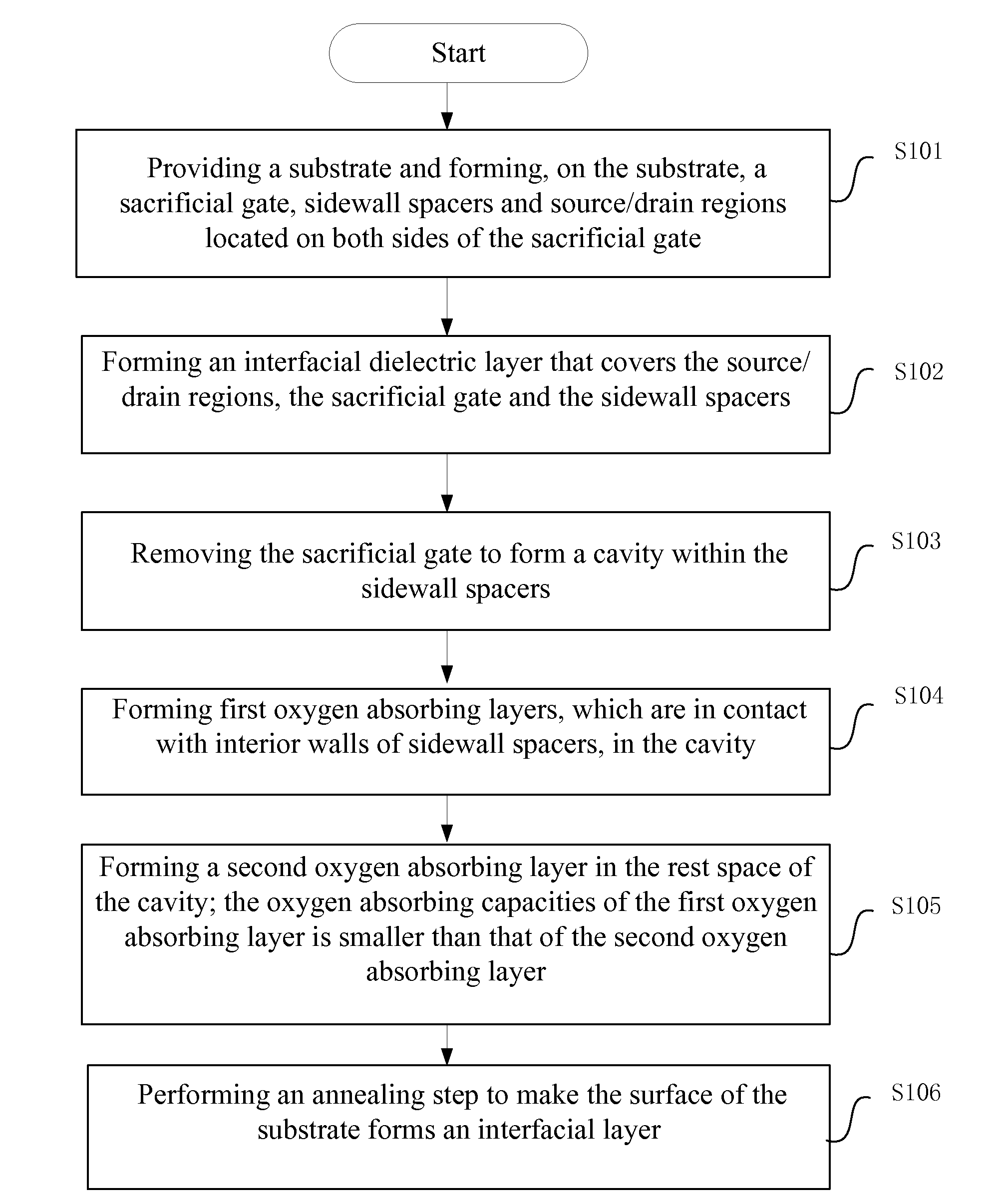
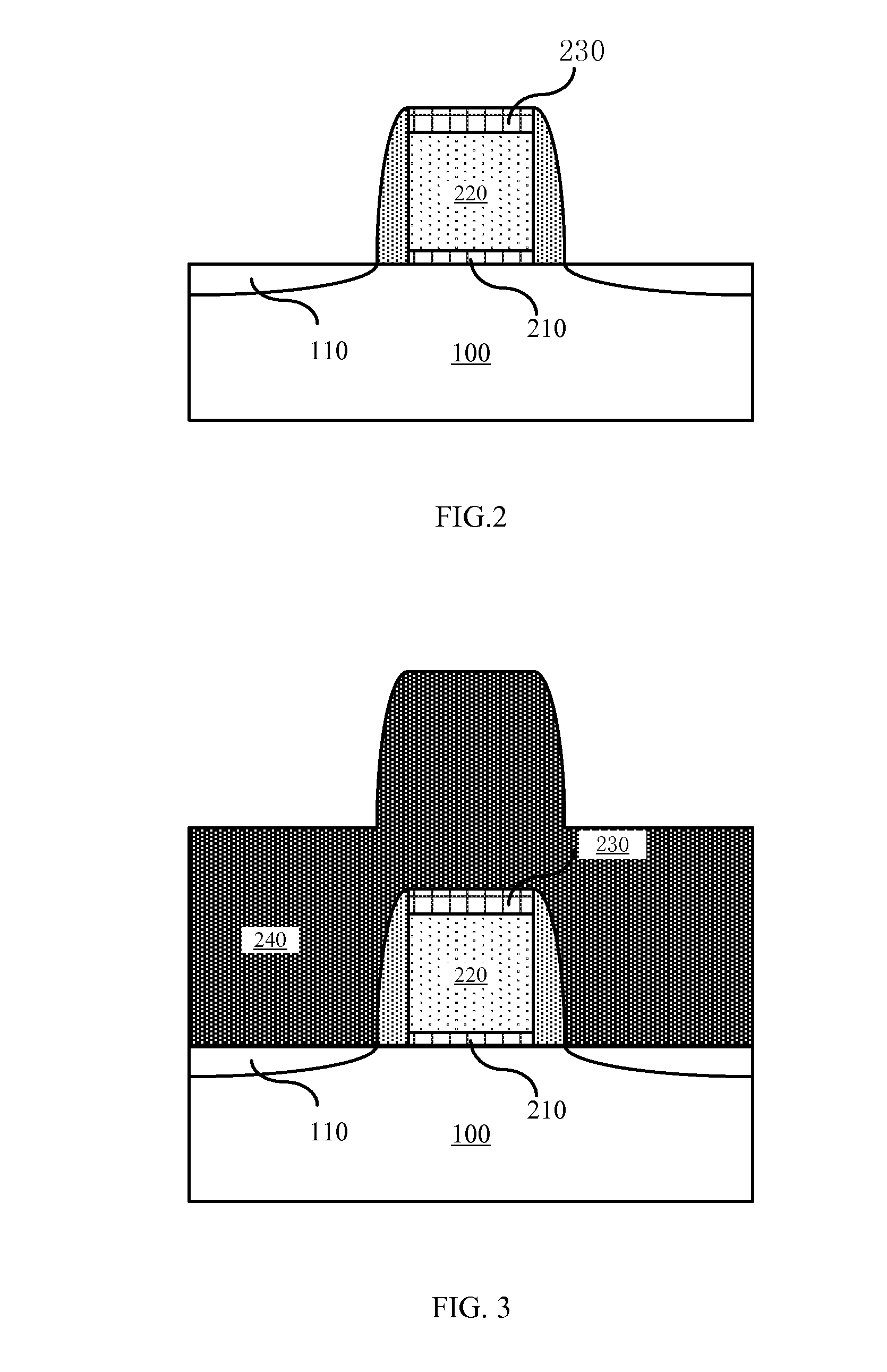
[0030]Referring to FIG. 8, FIG. 8 illustrates a cross-sectional view of a semiconductor structure in accordance with the aspects of the present invention. The semiconductor structure comprises a substrate 100, source / drain regions 110, a gate stack and an interfacial layer, wherein

[0031]the substrate 100 has a channel region;

[0032]the source / drain regions 110 are formed in the substrate 100 and located on both sides of the channel region;

[0033]the gate stack comprises a high-k dielectric layer 210 and a gate located on the high-k dielectric layer 210; the high-k dielectric layer 210 is located on the channel region; wherein, the gate comprises first oxygen absorbing layers 250 and a second oxygen absorbing layer 260; the first oxygen absorbing layers 250 are formed to surround the sidewalls of the second oxygen absorbing layer 260, and the oxygen absorbing capacities of the first oxygen absorbing layers 250 is less than that of the second oxygen absorbing layer 260.

[0034]An interfac...


PUM


Abstract

The present invention provides a semiconductor structure and a method for manufacturing the same. The method comprises the following steps: providing a substrate and forming a sacrificial gate, sidewall spacers and source/drain regions located on both sides of the sacrificial gate; forming an interlayer dielectric layer that covers the device; removing the sacrificial gate to form a cavity within the sidewall spacers; forming first oxygen absorbing layers in the cavity; forming a second oxygen absorbing layer in the remaining of the space of the cavity; and performing an annealing step to make the surface of the substrate form an interfacial layer. The present invention further provides a semiconductor structure. By forming a symmetrical interfacial layer in a channel region, the present invention has reduced processing difficulty while effectively mitigating short-channel effects and preserving carrier mobility.

Description

[0001]The present application claims priority to Chinese Patent application No. 2011103068854, filed on Oct. 11, 2011, entitled “SEMICONDUCTOR STRUCTURE AND METHOD FOR MANUFACTURING THE SAME”, which is incorporated herein by reference in its entirety.FIELD OF THE INVENTION[0002]The present invention relates to the field of semiconductor manufacturing, and particularity, to a semiconductor structure and a method for manufacturing the same.BACKGROUND OF THE INVENTION[0003]With the developing of the semiconductor industry, the integrated circuits having more advanced performance and more powerful functions require greater component density. Size of each part and component, together with the space there between, will need to be further scaled down (Today, the dimensions of the components and space therebetween have already reached to nanometer scale). Therefore the demand for increasing density of components in a semiconductor device imposes more stringent requirements on the process co...

Claims


Application Information

Patent Timeline
IPC IPC(8): H01L29/66H01L29/78
CPCH01L29/66545H01L29/78H01L21/28176H01L29/66553H01L29/66575H01L29/42368H01L29/513H01L29/518
Inventor YIN, HAIZHOUYU, WEIZE
Owner INST OF MICROELECTRONICS CHINESE ACAD OF SCI
Why Eureka
Try Eureka