Method and apparatus for germanium tin alloy formation by thermal CVD

a technology of germanium tin alloy and thermal cvd, which is applied in the direction of crystal growth process, polycrystalline material growth, chemically reactive gas, etc., can solve the problems of less resistivity, less electronic properties of channels, and increased threshold voltage, so as to improve selective deposition on semi-conductive regions of substrates.

Inactive Publication Date: 2013-10-24
APPLIED MATERIALS INC
View PDF2 Cites 280 Cited by
  • Summary
  • Abstract
  • Description
  • Claims
  • Application Information

AI Technical Summary

Problems solved by technology

As device geometries decline according to Moore's Law, the size of transistor components poses challenges to engineers working to make devices that are smaller, faster, use less power, and generate less heat.
For example, as the size of a transistor declines, the channel region of the transistor becomes smaller, and the electronic properties of the channel become less viable, with more resistivity and higher threshold voltages.

Method used


Image

  • Method and apparatus for germanium tin alloy formation by thermal CVD
  • Method and apparatus for germanium tin alloy formation by thermal CVD
  • Method and apparatus for germanium tin alloy formation by thermal CVD

Examples


Embodiment Construction

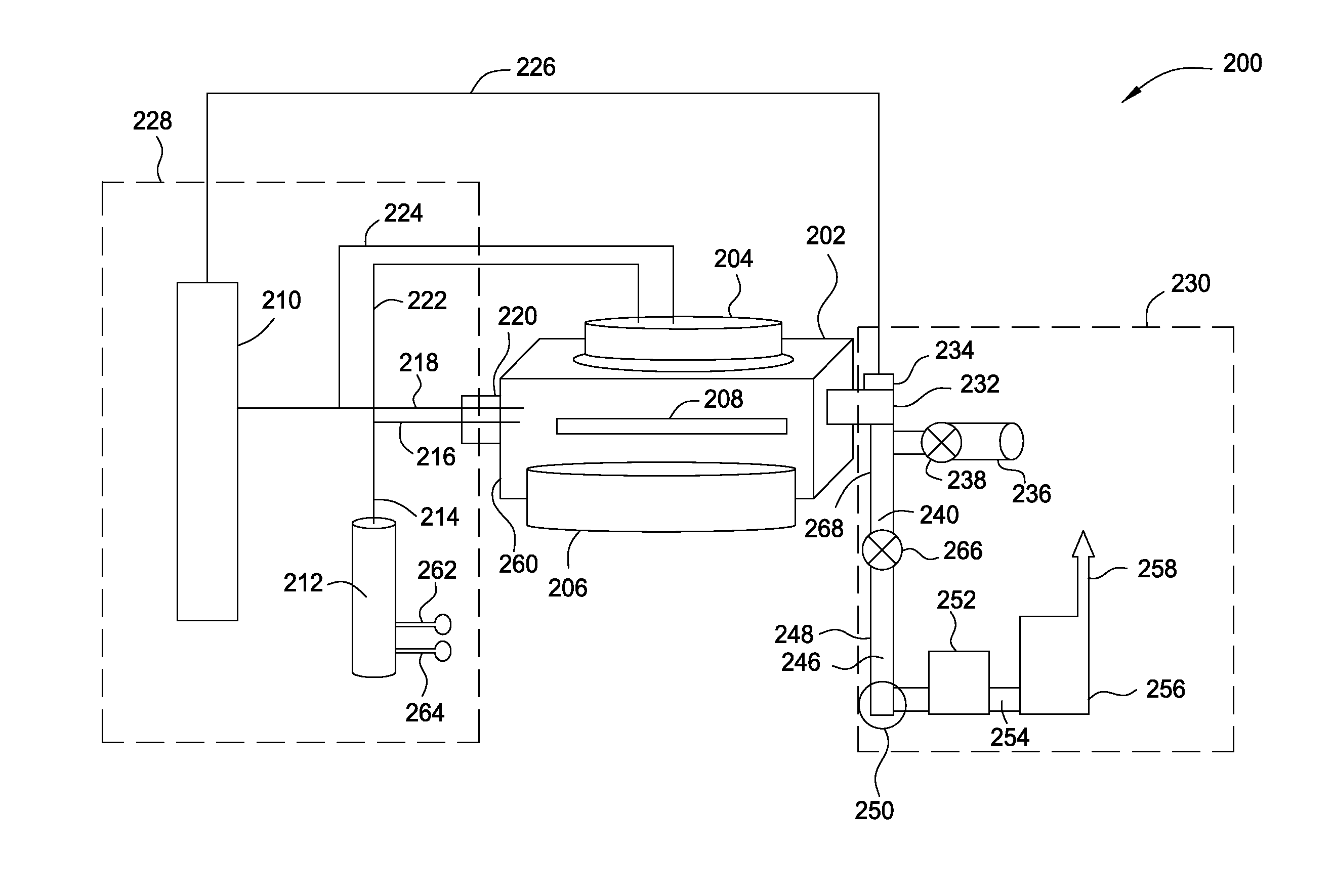
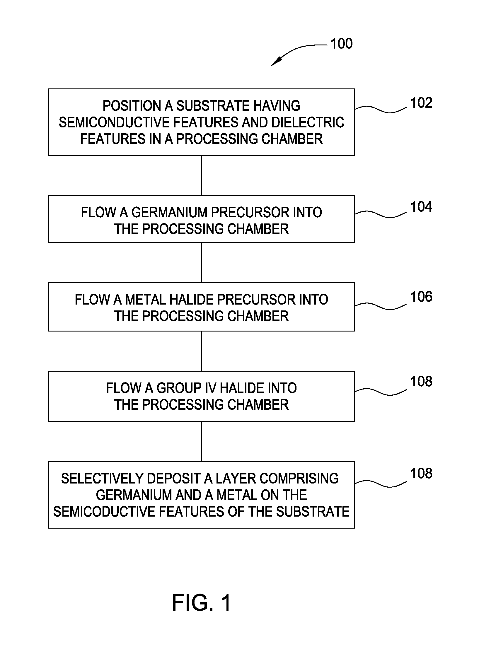
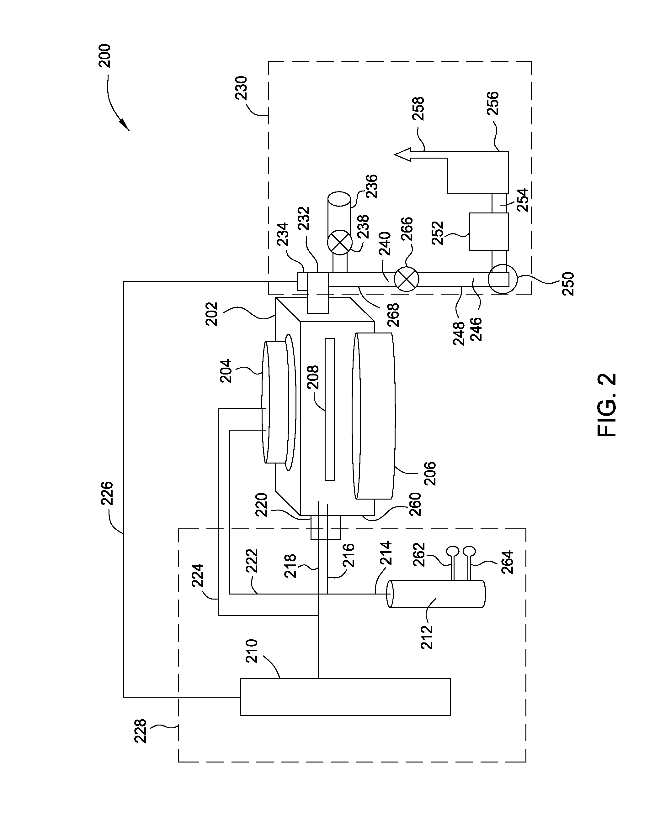
[0016]FIG. 1 is a flow diagram summarizing a method 100 according to one embodiment. A semiconductor substrate is positioned in a processing chamber at 102. The semiconductor substrate may be any semiconductive material on which a group IV semiconductive semiconductor-alloy layer is to be formed. A silicon substrate on which a transistor structure is to be formed may be used in one example. The substrate may have any known semiconductive materials, such as silicon, germanium, carbon, group III / V semiconductor materials, group II / VI semiconductor materials, and combinations or mixtures thereof. For example, the substrate may have silicon areas and germanium areas. The substrate may also have areas that are a mixture of silicon and germanium.

[0017]The semiconductor substrate may also have dielectric areas formed on a surface thereof. For example, a silicon substrate may have transistor gate structures and dielectric spacers formed adjacent to semiconductive source / drain regions, which...


PUM

PropertyMeasurementUnit
temperatureaaaaaaaaaa

Abstract

A method and apparatus for forming semiconductive semiconductor-metal alloy layers is described. A germanium precursor and a metal precursor are provided to a chamber, and an epitaxial layer of germanium-metal alloy, optionally including silicon, is formed on the substrate. The metal precursor is typically a metal halide, which may be provided by evaporating a liquid metal halide, subliming a solid metal halide, or by contacting a pure metal with a halogen gas. A group IV halide deposition control agent is used to provide selective deposition on semiconductive regions of the substrate relative to dielectric regions. The semiconductive semiconductor-metal alloy layers may be doped, for example with boron, phosphorus, and / or arsenic. The precursors may be provided through a showerhead or through a side entry point, and an exhaust system coupled to the chamber may be separately heated to manage condensation of exhaust components.

Description

CROSS-REFERENCE TO RELATED APPLICATIONS[0001]This application claims benefit of U.S. provisional patent application Ser. No. 61 / 635,978, filed Apr. 20, 2013, which is herein incorporated by reference.BACKGROUND OF THE INVENTION[0002]1. Field of the Invention[0003]Technology described herein relates to manufacture of semiconductor devices. More specifically, methods are described of forming group IV semiconductive semiconductor-metal alloy layers in both field effect transistors and photonic devices such as lasers.[0004]2. Description of the Related Art[0005]Germanium was one of the first materials used for semiconductor applications such as CMOS transistors. Due to vast abundance of silicon compared to germanium, however, silicon has been the overwhelming semiconductor material of choice for CMOS manufacture. As device geometries decline according to Moore's Law, the size of transistor components poses challenges to engineers working to make devices that are smaller, faster, use les...

Claims


Application Information

Patent Timeline
Patent Type & Authority Applications(United States)
IPC IPC(8): H01L21/02
CPCH01L21/0262C30B25/02C30B29/06C30B29/08C30B29/52H01L21/02524H01L21/02532H01L21/02535
Inventor KIM, YIHWANHUANG, YI-CHIAUSANCHEZ, ERROL ANTONIO C.
Owner APPLIED MATERIALS INC
Why Eureka
Try Eureka