

Microfluidic chip for susceptibility of superparamagnetic nanoparticles of bead and droplet types and measuring method for susceptibility using the same
a microfluidic chip and superparamagnetic nanoparticle technology, applied in the field of microfluidic chips, can solve the problems of high cost, unsuitable use method, unsuitable point-of-care testing, etc., and achieve the effect of high accuracy
- Summary
- Abstract
- Description
- Claims
- Application Information
AI Technical Summary
Benefits of technology
Problems solved by technology
Method used
Image

Examples
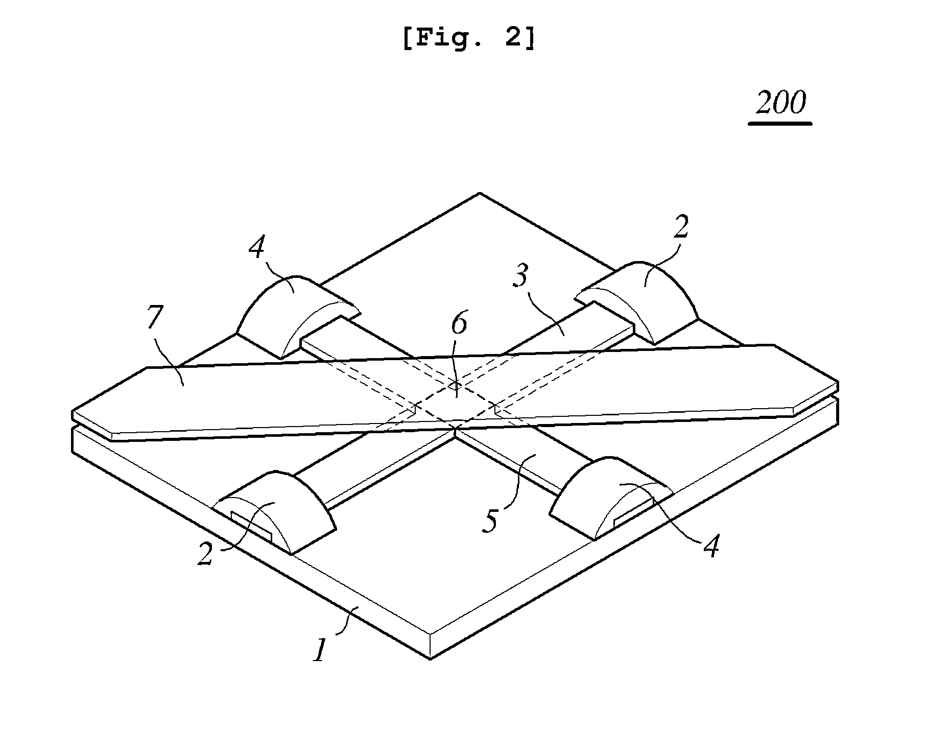
example 1
Fabrication of Planar Hall Resistive Sensor
[0126]A planar Hall resistive sensor was fabricated on a glass substrate having a size of 30 mm×30 mm by repeating photolithographic and sputtering processes.
[0127]1. Photolithography
[0128]Photoresist (Az 5214, AZ Electronic Materials) was dropped onto a glass substrate, after which it was spin-coated using a spin coater at 3000 RPM for 30 seconds and heat-treated at 120° C. for 1 minute. A mask was aligned on the heat-treated substrate using a mask aligner (MDA 400S, MIDAS SYSTEM. Korea), followed by exposure to light for 10 seconds. The exposed substrate was developed with an AZ developer for 1 minute, and then washed in distilled water.
[0129]2. Deposition of Planar Hall Resistive Sensor by Sputter
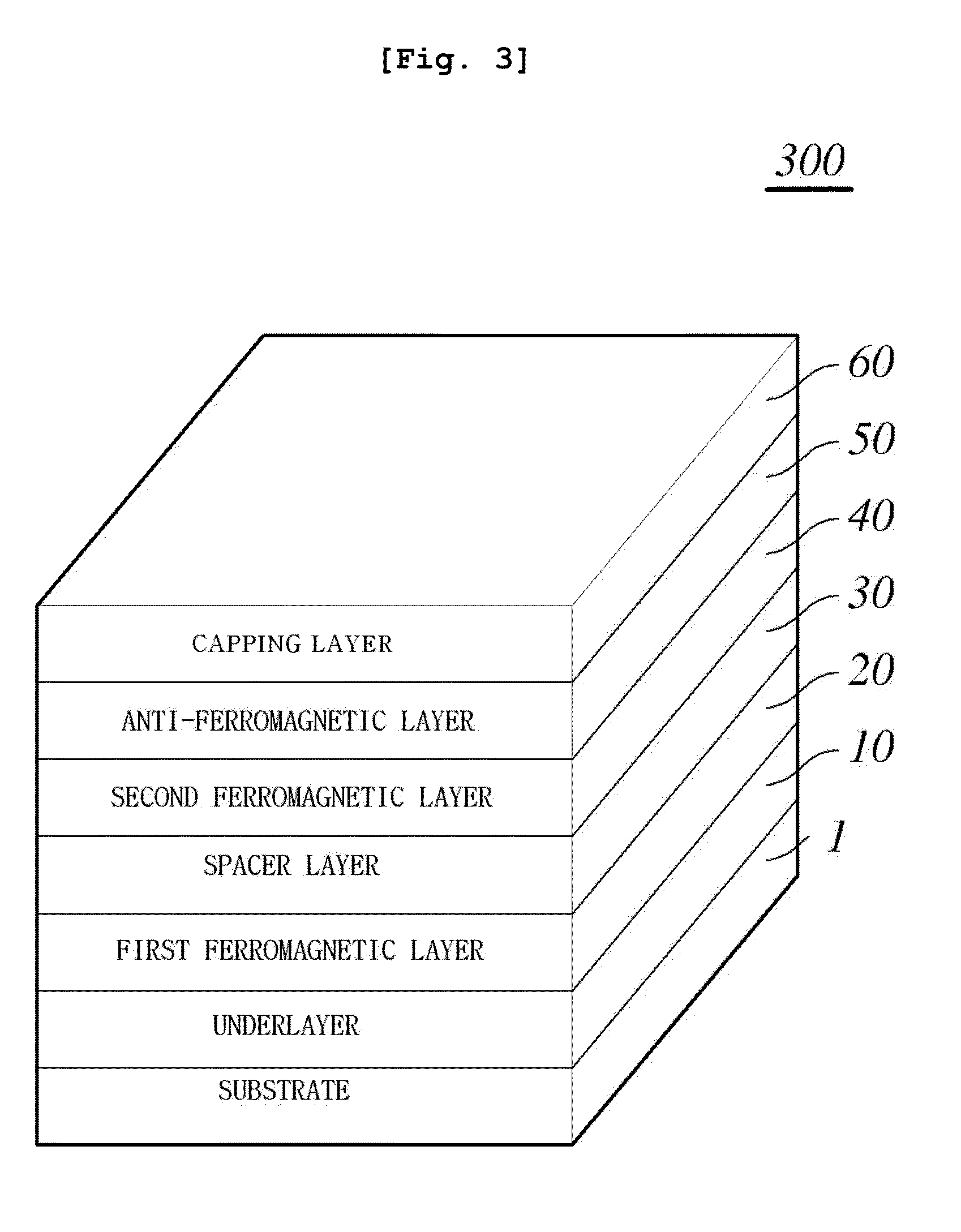
[0130]After the photolithographic process, the substrate was placed in a magnetron sputter, and a sensor layer was deposited on the substrate. The sensor had a spin valve structure consisting of Ta (6 nm), nickel-iron (NiFe) (10 nm), Cu (1.2 nm)...
example 2
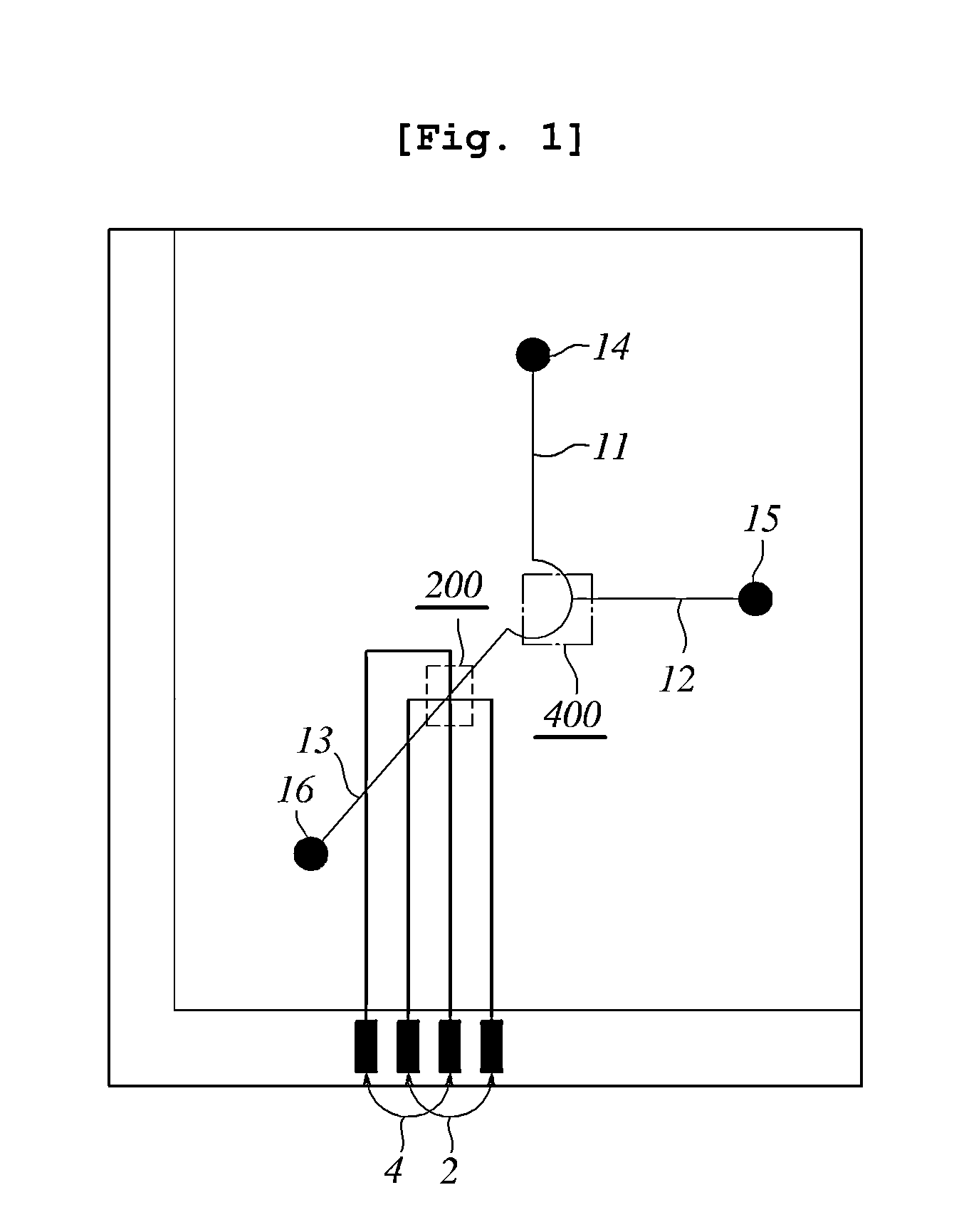
Fabrication of Microfluidic Chip
[0131]1. Formation of Microfluidic Channels
[0132]1-1. Fabrication of Mold by Photolithography
[0133]First, a mold was fabricated on a 3 inch silicon substrate by a photolithographic process. The silicon substrate used had a 500 nm thick SiO2 layer at one side and was ultrasonically washed with acetone for 30 min and methanol for 30 min. SU-8 2015 (MICROCHEM) photoresist was spin-coated on the washed silicon substrate to a thickness of 10 μm using a spin coater (SPIN 1200D, MIDAS SYSTEM. Korea) at 2000 RPM. The photoresist-coated substrate was heat-treated in an oven at 70° C. for 2 minutes, and then heat-treated in an oven at 100° C. for 5 minutes. A mask was aligned on the heat-treated substrate in a mask aligner, and then exposed to light for 5 minutes. After exposure to light, the substrate was heat-treated in an oven at 70° C. for 1 minute, and then heat-treated in an oven at 100° C. for 2 minutes. The heat-treated substrate was developed in an SU ...
example 3
Measurement of Magnetic Susceptibility of Superparamagnetic Nanoparticle Bead Using Microfluidic Chip
[0138]1. Measurement of Magnetic Fluid Flowing in Microfluidic Chip
[0139]In order to measure a magnetic fluid flowing in the microfluidic chip under visual observation, a microscope was placed on a Helmholtz coil and connected to a monitor. In order to accurately measure a signal when a magnetic fluid flowing in the channel passes over the sensor, a microscopic program capable of observing the movement of the magnetic fluid and a Labview program capable of measuring the change in the signal in the sensor were provided in a single computer, and a system was designed such that two sets of data could be simultaneously observed on a single monitor. The microfluidic chip including the planar Hall resistive sensor was located at the center of a Helmholtz coil. The profile of the planar Hall resistive sensor was measured, and a magnetic field corresponding to the highest sensitivity of the ...
PUM
 Abstract
Description
Claims
Application Information