Structure and Method for Inductors Integrated into Semiconductor Device Packages

a technology of semiconductor devices and inductors, applied in the direction of inductance, magnetic core inductance, inductance/solid-state device details, etc., can solve the problems of field energy levels needing to be modified, product parts such as dc-dc power supplies with bulky and relatively expensive three-dimensional inductors, etc., and achieve the effect of low cos

Inactive Publication Date: 2013-11-21
TEXAS INSTR INC
View PDF5 Cites 30 Cited by
  • Summary
  • Abstract
  • Description
  • Claims
  • Application Information

AI Technical Summary

Benefits of technology

[0012]It is a technical advantage of the invention that the fabrication of the inductors need only low cost common package manufacturing processes and equipment. It is another technical advantage that the inductors of the invention can be integrated into the packages as part of the slim device dimensions.
[0013]As an example, a

Problems solved by technology

As a consequence, he saw that product parts such as DC-DC power supplies with bulky and relatively costly three-dimensional indu

Method used


Image

  • Structure and Method for Inductors Integrated into Semiconductor Device Packages
  • Structure and Method for Inductors Integrated into Semiconductor Device Packages
  • Structure and Method for Inductors Integrated into Semiconductor Device Packages

Examples


Embodiment Construction

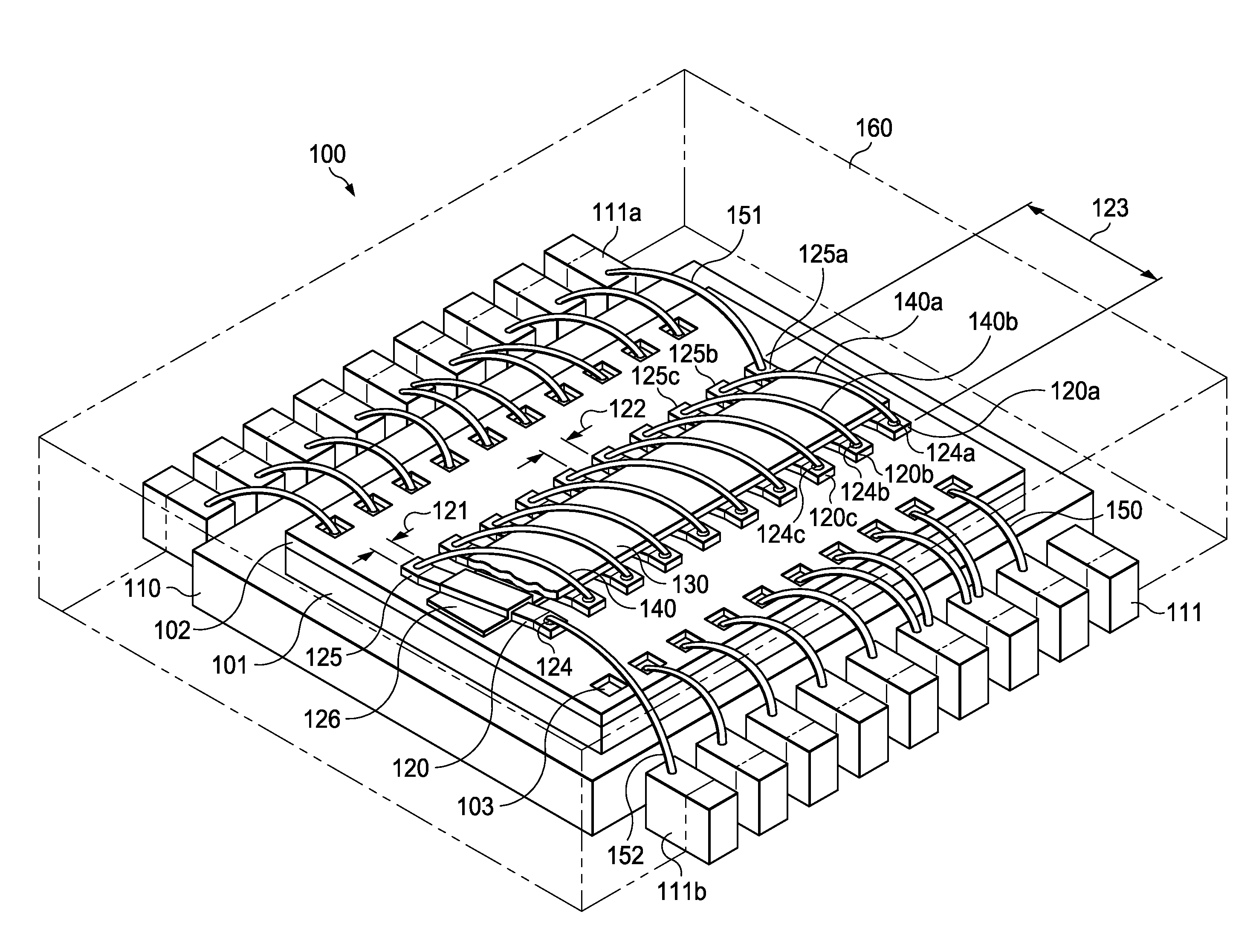
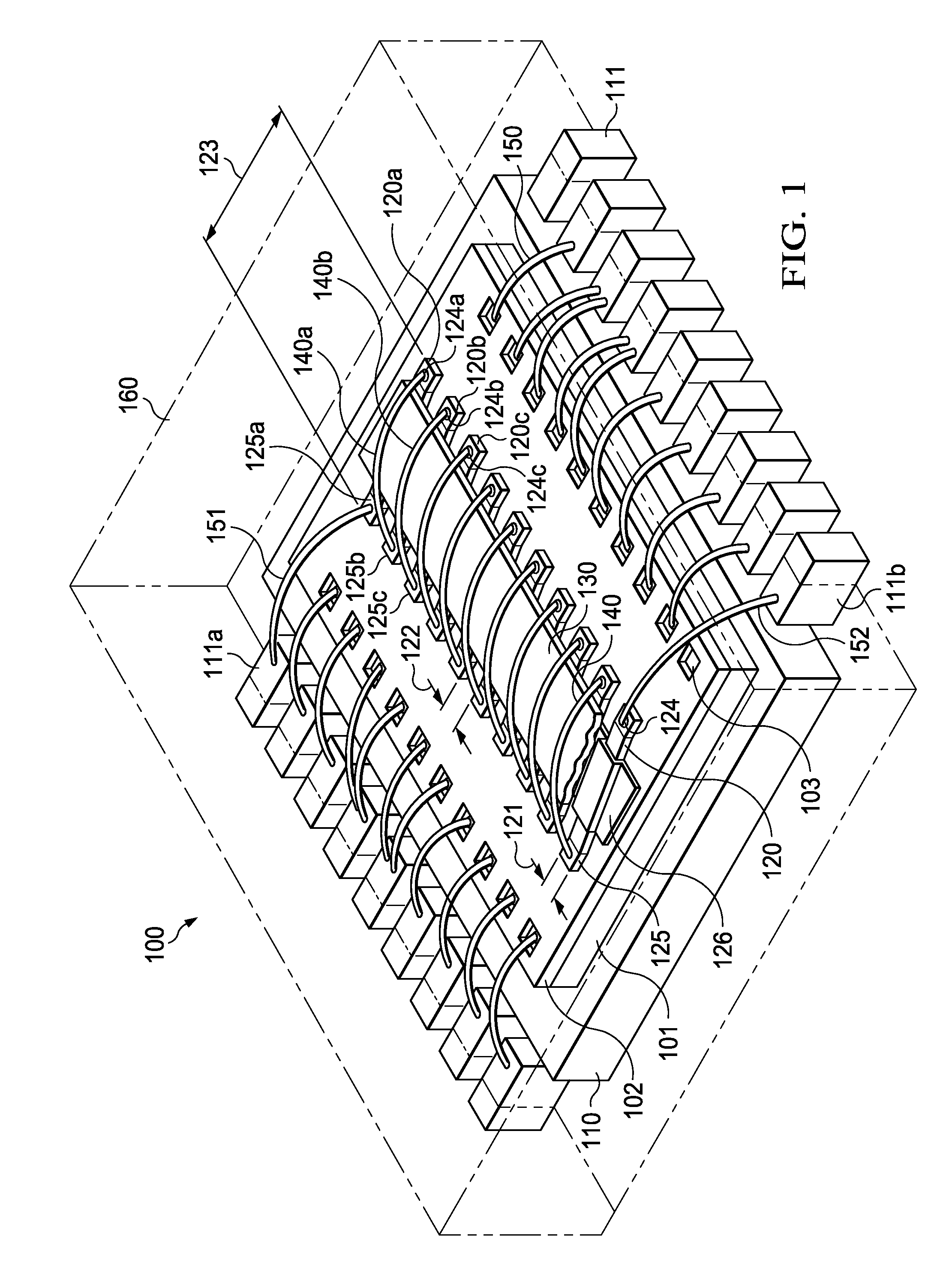
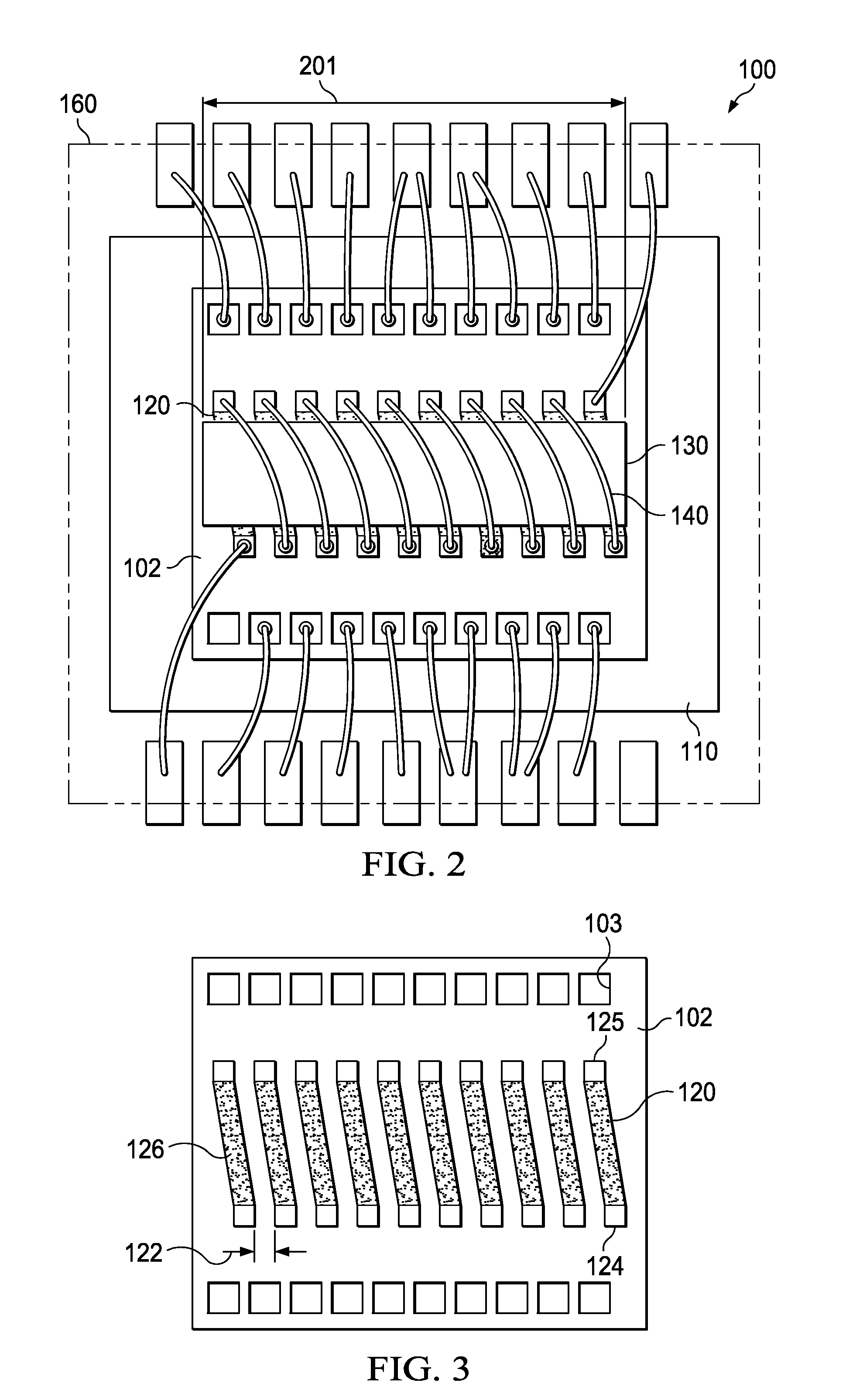
[0023]The exemplary embodiment of the invention illustrated in FIG. 1 and generally designated 100 shows a solenoid integrated into the package of a semiconductor device according to the invention. A semiconductor chip 101, for instance made of silicon, has a dielectric layer 102, for instance silicon oxynitride, over its integrated circuitry. The terminals 103 of the circuitry are not covered by the dielectric layer so that electrical contacts can be affixed to the circuitry; in the exemplary device 100, the terminals are realized as bond pads. Preferred bond pad metals include aluminum, or a stack of nickel and gold. Chip 101 is attached to a substrate 110. In the example of FIG. 1, substrate 110 is shown as the chip pad of a metallic leadframe, but in other devices substrate 110 may be a laminated multi-metal layer composite or another suitable insulating carrier. The chip attachment layer, for instance an adhesive polymer material, is not shown in FIG. 1.

[0024]Laying flat on the...


PUM


Abstract

A thin-contour semiconductor device with a solenoid and iron core integrated into the device package. The solenoid windings are constructed by a stripe-shaped layer portion, deposited on the chip surface, and an arced wire portion welded to the layer portion by low-cost standard wire bonding technique. The stripes are arrayed parallel to each other, spaced apart respective insulating gaps. The arced wires span from one stripe to the adjacent next stripe by bridging the gap and keeping the clock direction constant. The arced solenoid windings are then integrated into the encapsulating device package. The ferromagnetic core may be shaped as a ring to allow the formation of a strong and nearly homogeneous magnetic field inside the solenoid, providing reliable energy storage for power supply circuits.

Description

FIELD[0001]Embodiments of the invention relate in general to the field of semiconductor devices and processes, and more specifically to the structure and fabrication method of semiconductor integrated circuit devices, which integrate the inductors of the circuits into the package of the devices.DESCRIPTION OF RELATED ART[0002]Inductors are essential elements for RF design. Based on planar spiral inductor models first published in 1996 and on the high level of semiconductor technology and device production, planar spiral inductors and planar solenoidal inductors of a wide variety of thin-film single-layered and double-layered designs are available in electronic products with integrated circuits (IC) for RF application. The inductors of these semiconductor products realize the needed inductances by silicon on-chip thin-film spiral and solenoidal designs incorporated into the two-dimensional layout of ICs. Since the inductance of an inductor is proportional to the magnetic permeability...

Claims


Application Information

Patent Timeline
IPC IPC(8): H01L29/86H01L21/02H01L21/56H01F5/00
CPCH01F17/0006H01F17/04H01F2017/0086H01F2027/2814H01L23/3107H01L23/495H01L23/5227H01L23/645H01L24/45H01L24/48H01L24/49H01L28/10H01L2224/05554H01L2224/45014H01L2224/45015H01L2224/45144H01L2224/45147H01L2224/48091H01L2224/4813H01L2224/48247H01L2224/49113H01L2924/00014H01L2924/1461H01L2924/181H01L2924/19042H01L2924/19104H01L2924/30107H01L2924/00H01L2924/00012H01L2924/20751H01L2924/20752H01L2924/20753H01L2924/206
Inventor KODURI, SREENIVASAN
Owner TEXAS INSTR INC
Why Eureka
Try Eureka