Organic electroluminescence element and illumination device

Inactive Publication Date: 2013-11-28
KONICA MINOLTA INC
View PDF3 Cites 6 Cited by
  • Summary
  • Abstract
  • Description
  • Claims
  • Application Information

AI Technical Summary

Benefits of technology

The present invention provides an organic electroluminescence element and an illumination device with improved productivity and decreased driving voltage.

Problems solved by technology

Hence, waveguide loss of surface plasmon mode light is large, and accordingly the light extraction efficiency does not increase.
One of the problems of the top emission type organic EL element is damaging the organic layers in a process of forming a transparent conductive layer, which lowers the light emission efficiency, increases a voltage and shortens life of the element, for example.
In particular, the above problem is conspicuous when a sputtering method having high productivity is used as the process of forming the transparent conductive layer.
Thus, it is a great challenge to balance productivity with element characteristics of the top emission type organic EL element.
However, because copper phthalocyanine, which has low transmittance, is used as the material of the transparent protective layer, the light emission efficiency decreases, which is a weakness of the technology.
Hence, it is effective in preventing oxidation damage to the organic layers in the sputtering process, but has the problem that the voltage increases by oxidation of the transparent protective layer.
When the transparent protective layer is thick, the problem that the voltage increases by oxidation of the transparent protective layer in the sputtering process becomes bigger.

Method used


Image

  • Organic electroluminescence element and illumination device
  • Organic electroluminescence element and illumination device
  • Organic electroluminescence element and illumination device

Examples


example 1

[0233]>

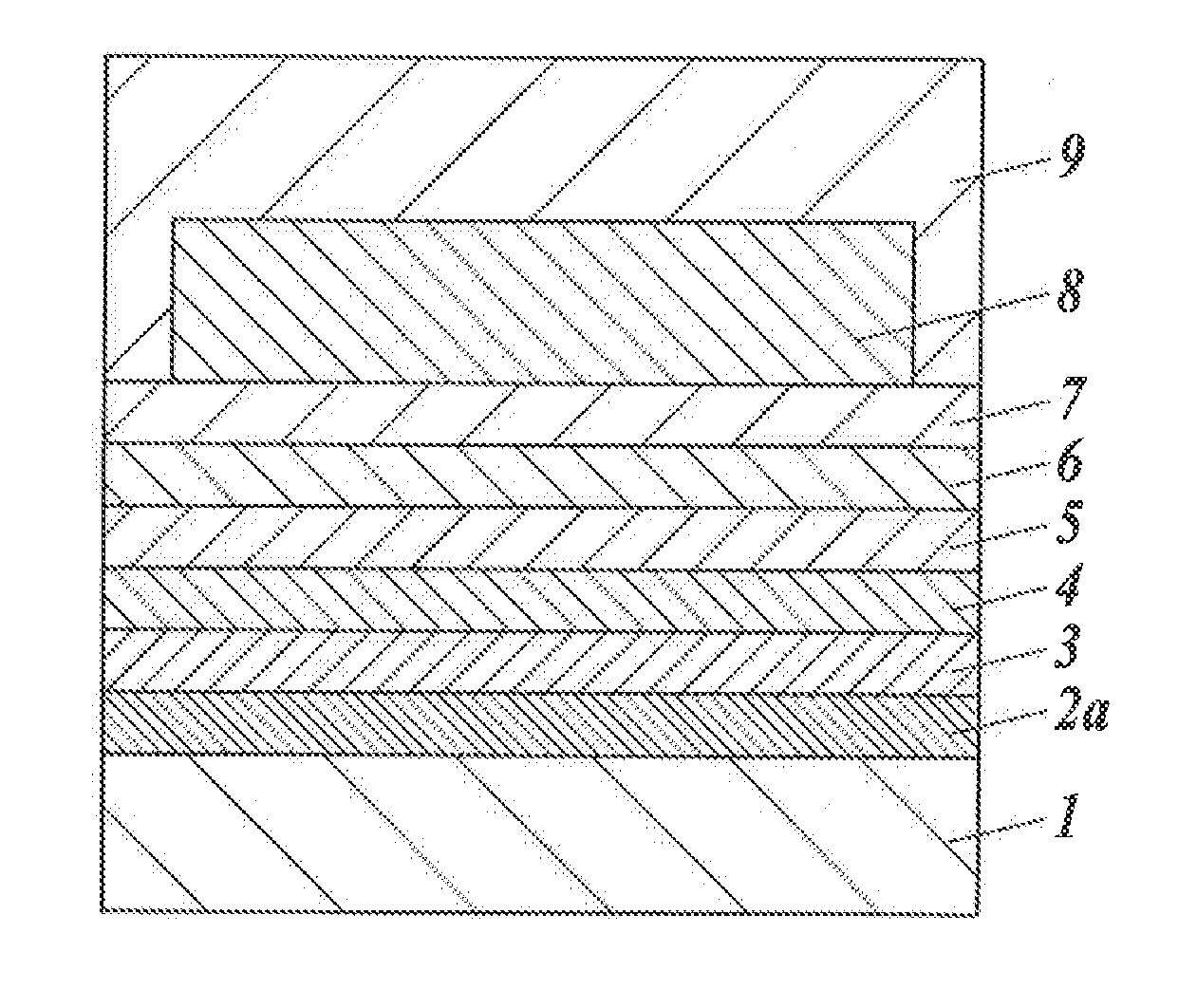
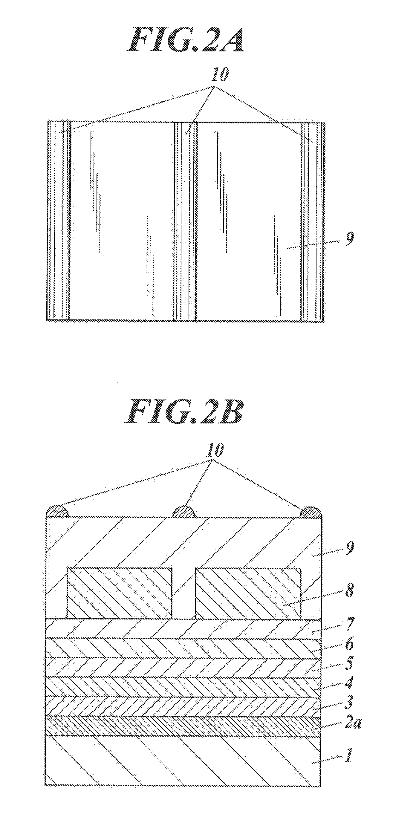
[0234]Organic El elements 1-1 to 1-26 were each produced in such a way as to have a light emitting area of 5 cm×5 cm.

[0235][Production of Organic EL Element 1-1]

[0236](Formation of Anode)

[0237]ITO was deposited on a transparent substrate 1 by sputtering under a condition of making the thickness thereof be 100 nm and then subjected to patterning, so that an anode constituted of an ITO layer was formed. Next, the substrate provided with the ITO layer was subjected to ultrasonic cleaning with isopropyl alcohol, dried with dry nitrogen gas, and then subjected to UV ozone cleaning for five minutes.

[0238](Formation of Positive Hole Injection Layer to Electron Transport Layer)

[0239]The substrate provided with the ITO layer was fixed onto a substrate holder of a commercial vacuum evaporation device. Then, the below-mentioned α-NPD, DPVBi, BAlq, Alq3 and potassium fluoride were placed in tantalum resistive heating boats, respectively, and the tantalum resistive heating boats were moun...

example 2

[0330]>

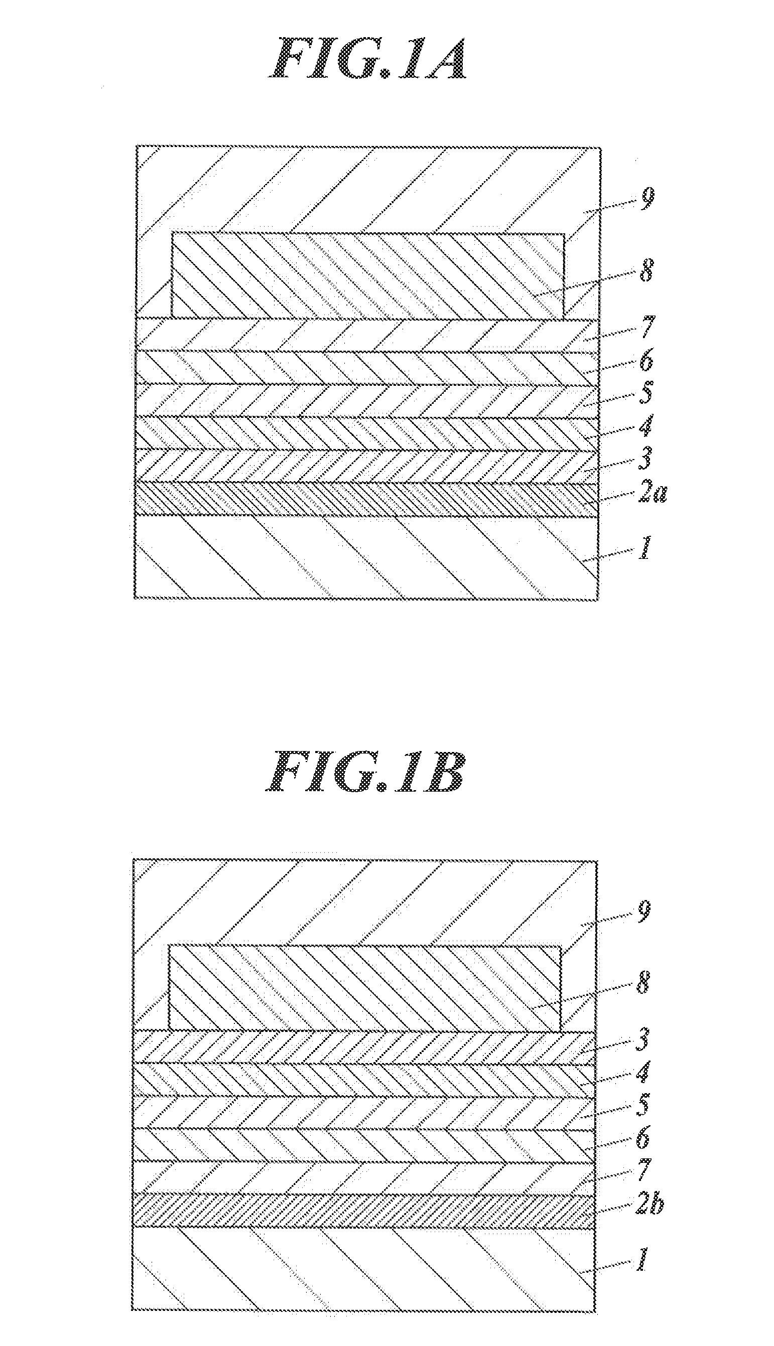
[0331]Organic El elements 2-1 to 2-23 were each produced in such a way as to have a light emitting area of 5 cm×5 cm.

[0332][Production of Organic EL Element 2-1]

[0333](Formation of Cathode)

[0334]Aluminum was deposited on a transparent substrate 1 by sputtering under a condition of making the thickness thereof be 100 nm and then subjected to patterning, so that an anode constituted of an aluminum layer was formed. Next, the substrate provided with the aluminum layer was subjected to ultrasonic cleaning with isopropyl alcohol, dried with dry nitrogen gas, and then subjected to UV ozone cleaning for five minutes.

[0335](Formation of Electron Injection Layer to Positive Hole Injection / Positive Hole Transport)

[0336]The substrate provided with the aluminum layer was fixed onto the substrate holder of the commercial vacuum evaporation device. Then, potassium fluoride, Alq3, BAlq, DPVBi and α-NPD were placed in tantalum resistive heating boats, respectively, and the tantalum resistive...


PUM


Abstract

An object is providing an organic electroluminescence element and an illumination device in which a driving voltage does not increase even when a high-productivity sputtering method is used to form a transparent conductive layer of the organic electroluminescence element of a top or top-and-bottom emission type, and hence which has an improved driving voltage. The organic electroluminescence element includes at least a light emitting layer and a transparent conductive layer. Between the light emitting layer and the transparent conductive layer, a transparent protective layer is disposed. The light emitting layer contains a phosphorescence emitting compound. The transparent protective layer contains a metal oxide. The metal oxide is a molybdenum (VI) oxide, a rhenium (VI) oxide or a nickel (II) oxide in an oxygen deficient state.

Description

TECHNICAL FIELD[0001]The present invention relates to an organic electroluminescence element and an illumination device applied to a display device, a lighting fixture and the like.BACKGROUND ART[0002]Recently, surface emitting bodies have attracted attention, the surface emitting bodies being used as backlights for various kinds of displays, display boards such as signboards and emergency lights, light sources for lighting fixtures and the like, because the surface emitting bodies have many advantages such as having high brightness, high light emission efficiency, small thickness and light weight. Among the surface emitting bodies, an organic electroluminescence element (hereinafter also called an organic EL element), which employs an organic material and emits light by electric energy from an anode and a cathode, has particularly attracted attention because the organic EL element can emit light at a low voltage of several volts to several ten volts, is of a thin-film type complete...

Claims


Application Information

Patent Timeline
IPC IPC(8): H01L51/00H01L51/50
CPCH01L51/0085H01L51/5012C07D213/79C07D221/10C07D233/58C07D401/14C07D405/14C07D409/14C07D417/14C07D471/04C07D519/00C09K11/06H05B33/10C09K2211/1007C09K2211/1011C09K2211/1014C09K2211/1029C09K2211/1033C09K2211/1044C09K2211/1048C09K2211/1059C09K2211/1088C09K2211/1092C09K2211/1096H10K85/6574H10K85/342H10K85/346H10K85/6572H10K50/11H10K2101/10H10K50/171H10K50/824H10K50/828H10K50/844H10K50/16H10K85/324H10K85/615H10K85/626H10K85/633
Inventor HAKII, TAKESHIISHIDAI, HIROSHI
Owner KONICA MINOLTA INC
Why Eureka
Try Eureka