

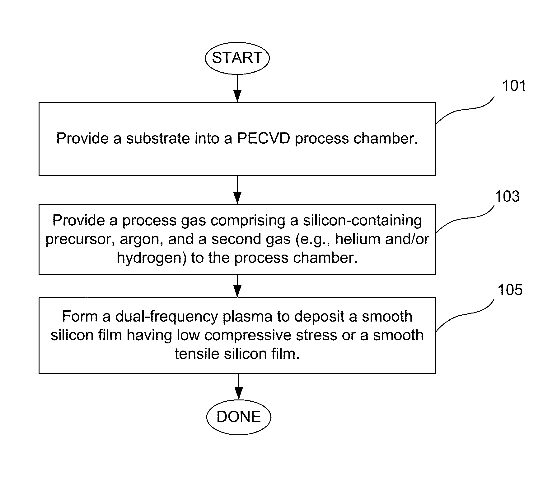
Pecvd deposition of smooth silicon films
a technology of smooth silicon and film, applied in the direction of liquid surface applicators, chemical vapor deposition coatings, coatings, etc., can solve the problems of difficult patterning of film stacks for three-dimensional (3d) memory devices, interfacial defects, and unacceptably rough top surface of film stacks for downstream patterning processes, etc., to achieve low compressive stress, low roughness, and low compressive stress
- Summary
- Abstract
- Description
- Claims
- Application Information
AI Technical Summary
Benefits of technology
Problems solved by technology
Method used
Image

Examples
example 1
[0039]In one experimentally validated example, a smooth silicon film was deposited at a temperature of 530° C. and at a pressure of 5.1 Torr from a process gas consisting essentially of silane (0.19% of total process gas volume), argon (38% of total process gas volume), helium (57% of total process gas volume), and hydrogen (4% of total process gas volume) using dual frequency plasma (13.56 MHz and 400 kHz), where LF power was at 50% of total power. The deposited smooth silicon film had Ra of 3.5 Å and a stress of −300 MPa.
example 2
[0040]In another experimental example, a smooth silicon film was deposited at a temperature of 530° C. and at a pressure of 5.1 Torr from a process gas consisting essentially of silane (0.19% of total process gas volume), argon (38% of total process gas volume), helium (57% of total process gas volume), and hydrogen (4% of total process gas volume) using dual frequency plasma (13.56 MHz and 400 kHz), where LF power was at 75% of total power. The deposited smooth silicon film had Ra of 4.2 Å and a stress of −280 MPa.
example 3
[0041]In another experimental example, a smooth silicon film was deposited at a temperature of 350° C. and at a pressure of 3 Torr from a process gas consisting essentially of silane (0.13% of total process gas volume), argon (33% of total process gas volume), and helium (66% of total process gas volume), using dual frequency plasma (13.56 MHz and 400 kHz), where LF power was at 17% of total power. The deposited smooth silicon film had Ra of 2.8 Å and a stress of −270 MPa.
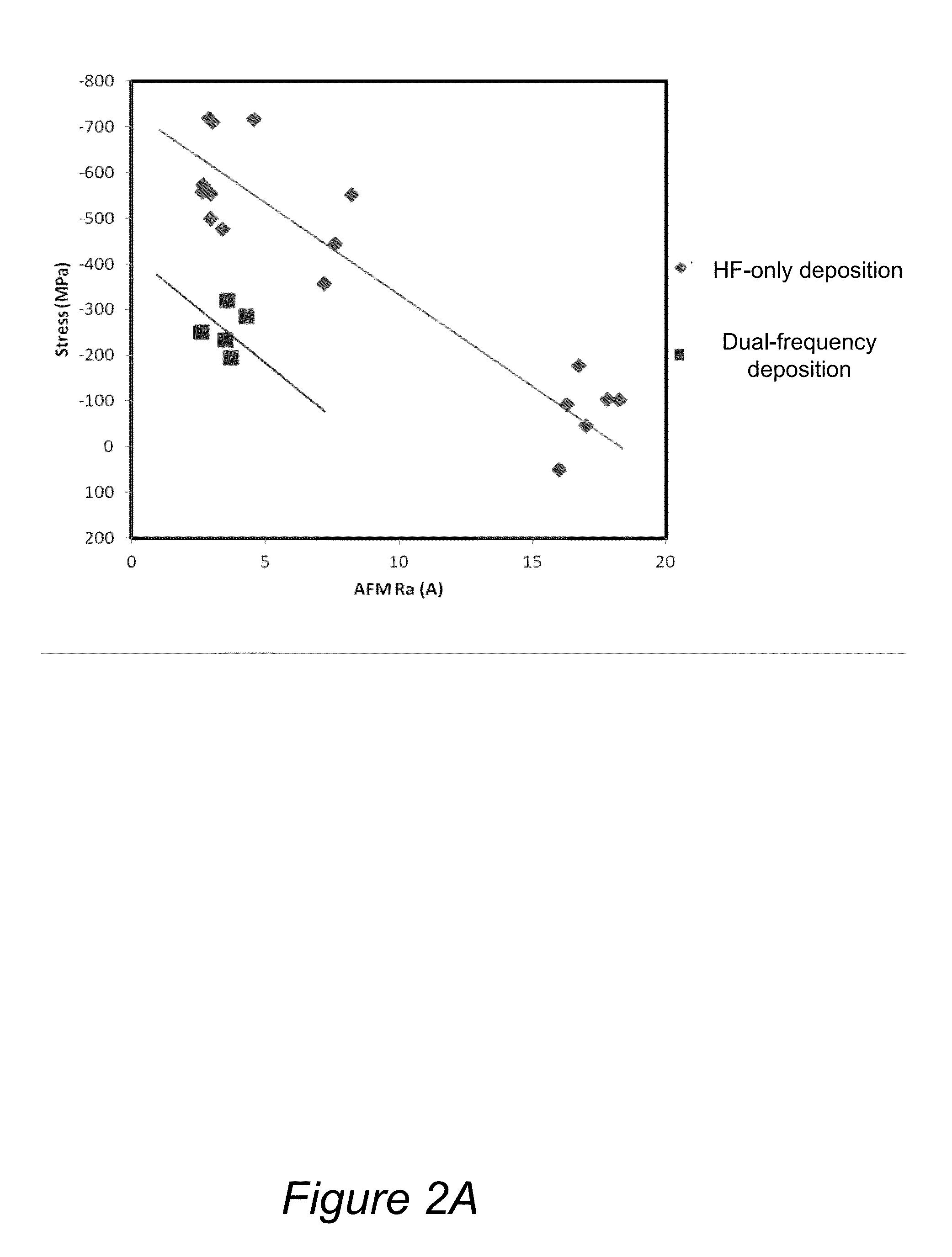
[0042]Another set of conditions, suitable for depositing smooth films having low compressive stress or smooth films having tensile stress is shown in Table 2. The films have an Ra of less than about 5 Å, and a compressive stress of less than 500 MPa in absolute value, including films having a compressive stress of less than 300 MPa in absolute value. Deposition is performed using a process gas consisting essentially of silane, argon, helium, and hydrogen using dual frequency plasma. The flow rates and power levels ...
PUM
| Property | Measurement | Unit |
|---|---|---|
| Fraction | aaaaa | aaaaa |
| Fraction | aaaaa | aaaaa |
| Fraction | aaaaa | aaaaa |
Abstract
Description
Claims
Application Information