Semiconductor device and method for manufacturing same

a technology of semiconductors and semiconductors, applied in the direction of semiconductor devices, bulk negative resistance effect devices, electrical appliances, etc., can solve the problems of deteriorating the adhesion between nickel and nickel, becoming impossible to achieve enhanced performance,

Inactive Publication Date: 2009-04-30
SONY CORP
View PDF4 Cites 14 Cited by
  • Summary
  • Abstract
  • Description
  • Claims
  • Application Information

AI Technical Summary

Benefits of technology

[0010]According to an embodiment of the present invention, there is provided a semiconductor device including an element isolation region configured to be formed in a semiconductor substrate, a P-type field effect transistor configured to be formed in a first element formation region of the semiconductor substrate for which isolation by the element isolation region is carried out, and an N-type substrate region configured to be formed in the semiconductor substrate for which isolation by the element isolation region is carried out. Arsenic is ion-implanted into the N-type substrate region. The semiconductor device further includes a nickel silicide layer configured to be formed on the N-type substrate region, a first insulating film configured to cover the P-type field effect transistor and have compressive stress, and a second insulating film configured to cover the N-type substrate region and have tensile stress or compressive stress lower than the compressive stress of the first insulating film.
[0011]In the semiconductor device according to this embodiment of the present invention, the N-type substrate region is covered by the second insulating film having tensile stress or compressive stress lower than that of the first insulating film covering the P-type field effect transistor. Therefore, although the density of the first insulating film is high, the density of the second insulating film is lower than that of the first insulating film. In particular, the density of the second insulating film having tensile stress is low. Therefore, even when an abnormal film (e.g. a film containing oxygen) is formed on the nickel silicide layer formed on the N-type substrate region in which arsenic is ion-implanted and water is absorbed by this abnormal film, the absorbed water will be discharged to the external via the second insulating film.
[0012]According to another embodiment of the present invention, there is provided a method for manufacturing a semiconductor device. The method includes the steps of forming in a semiconductor substrate an element isolation region that isolates a first element formation region, an N-type substrate region, a second element formation region, and a P-type substrate region from each other, turning a partial portion of the semiconductor substrate in the first element formation region and the N-type substrate region into an N-type region and turning a partial portion of the semiconductor substrate in the second element formation region and the P-type substrate region into a P-type region, and forming a P-type field effect transistor in the first element formation region and forming an N-type field effect transistor in the second element formation region. The method further includes the steps of forming a nickel silicide layer on the N-type substrate region after ion implantation of arsenic into the N-type substrate region, forming a first insulating film that covers the P-type field effect transistor and has compressive stress over the semiconductor substrate except the N-type substrate region, and forming a second insulating film that covers the N-type substrate region and has tensile stress or compressive stress lower than the compressive stress of the first insulating film.
[0013]In the method for manufacturing a semiconductor device according to this embodiment of the present invention, the N-type substrate region is covered by the second insulating film having tensile stress or compressive stress lower than that of the first insulating film covering the P-type field effect transistor. Therefore, although the density of the first insulating film is high, the density of the second insulating film is lower than that of the first insulating film. In particular, the density of the second insulating film having tensile stress is low. Therefore, even when an abnormal film (e.g. a film containing oxygen) is formed on the nickel silicide layer formed on the N-type substrate region in which arsenic is ion-implanted and water is absorbed by this abnormal film, the absorbed water will be discharged to the external via the second insulating film.
[0014]The semiconductor device according to the embodiment of the present invention allows water absorbed on the nickel silicide layer to be discharged to the external via the second insulating film, and thus has an advantage that the problem of film separation on the nickel silicide layer on the N-type substrate region can be solved.
[0015]The method for manufacturing a semiconductor device according to the embodiment of the present invention allows water absorbed on the nickel silicide layer to be discharged to the external via the second insulating film, and thus has an advantage that the problem of film separation on the nickel silicide layer on the N-type substrate region can be solved.

Problems solved by technology

However, for LSI devices of the 45-nm-generation and the subsequent generations, it is becoming impossible to achieve enhanced performance through mere size shrinking, due to the influence of the abrupt deterioration of the short-channel characteristic of MOSFETs, and so on.
This will significantly deteriorate the adhesion between the nickel silicide layer and a silicon nitride film as the CESL film.
Consequently, the problem that should be solved is that, if a dense film such as a compressive film is applied as a silicon nitride film, water absorbed by an abnormal oxide film formed on a nickel silicide layer is hardly discharged and thus separation occurs at the interface between the nickel silicide layer and the silicon nitride film.

Method used


Image

  • Semiconductor device and method for manufacturing same
  • Semiconductor device and method for manufacturing same
  • Semiconductor device and method for manufacturing same

Examples


first embodiment

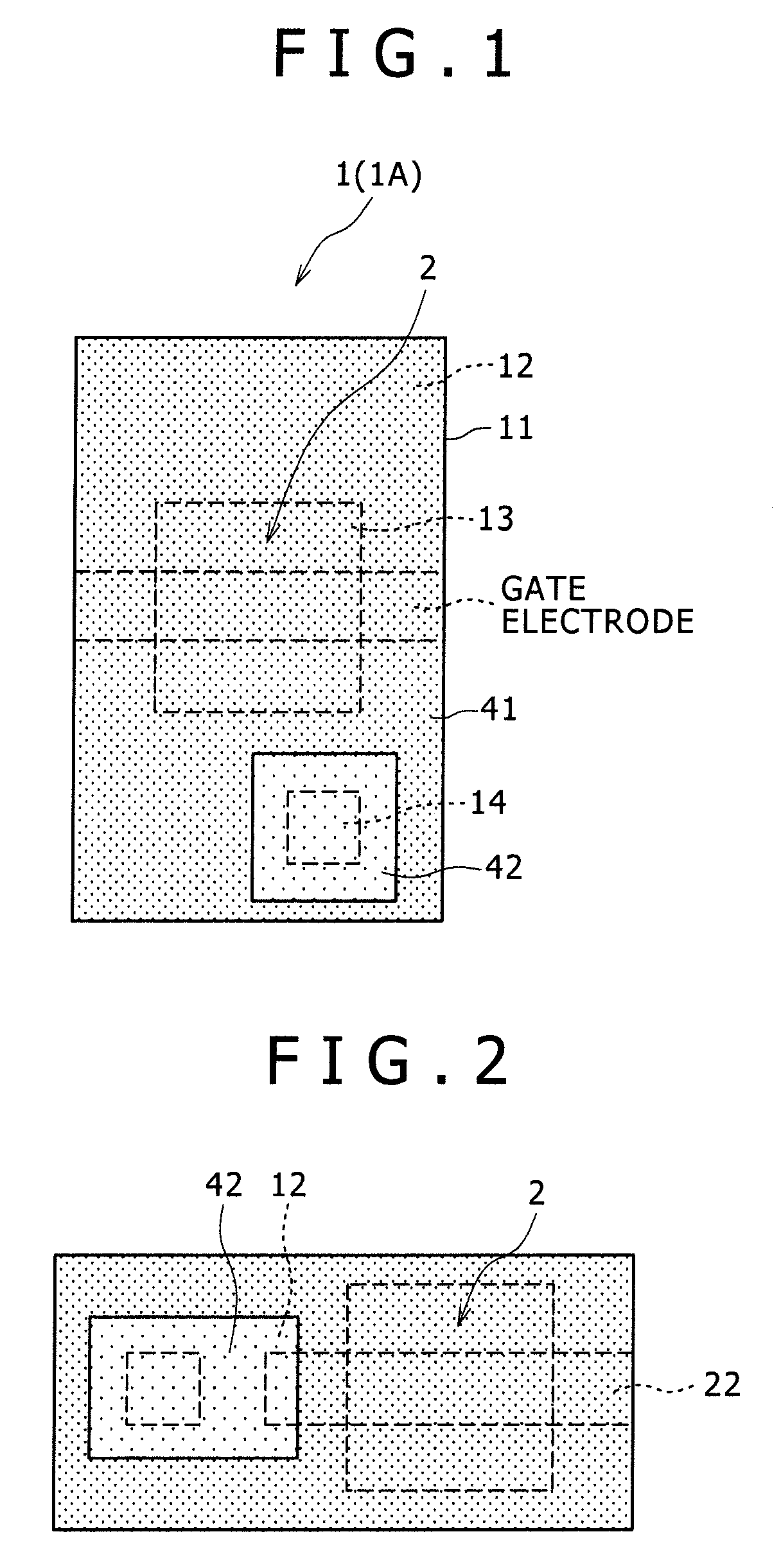
[0035]A semiconductor device according to one embodiment (first embodiment) of the present invention will be described below with reference to a layout plane view of FIG. 1.

[0036]As shown in FIG. 1, by an element isolation region 12 formed in a semiconductor substrate 11, a first element formation region 13 as the formation region of a P-type field effect transistor 2 and an N-type substrate region 14 serving as a contact region are isolate from each other.

[0037]The P-type field effect transistor 2 is formed in the first element formation region 13. In the N-type substrate region 14, arsenic is ion-implanted to a deep position (e.g. to a position deeper than the source and drain regions of the transistor). On this N-type substrate region 14, a nickel silicide layer (not shown) is formed e.g. across the entire surface of the N-type substrate region 14. By this ion implantation, an N-type region is formed in the N-type substrate region 14.

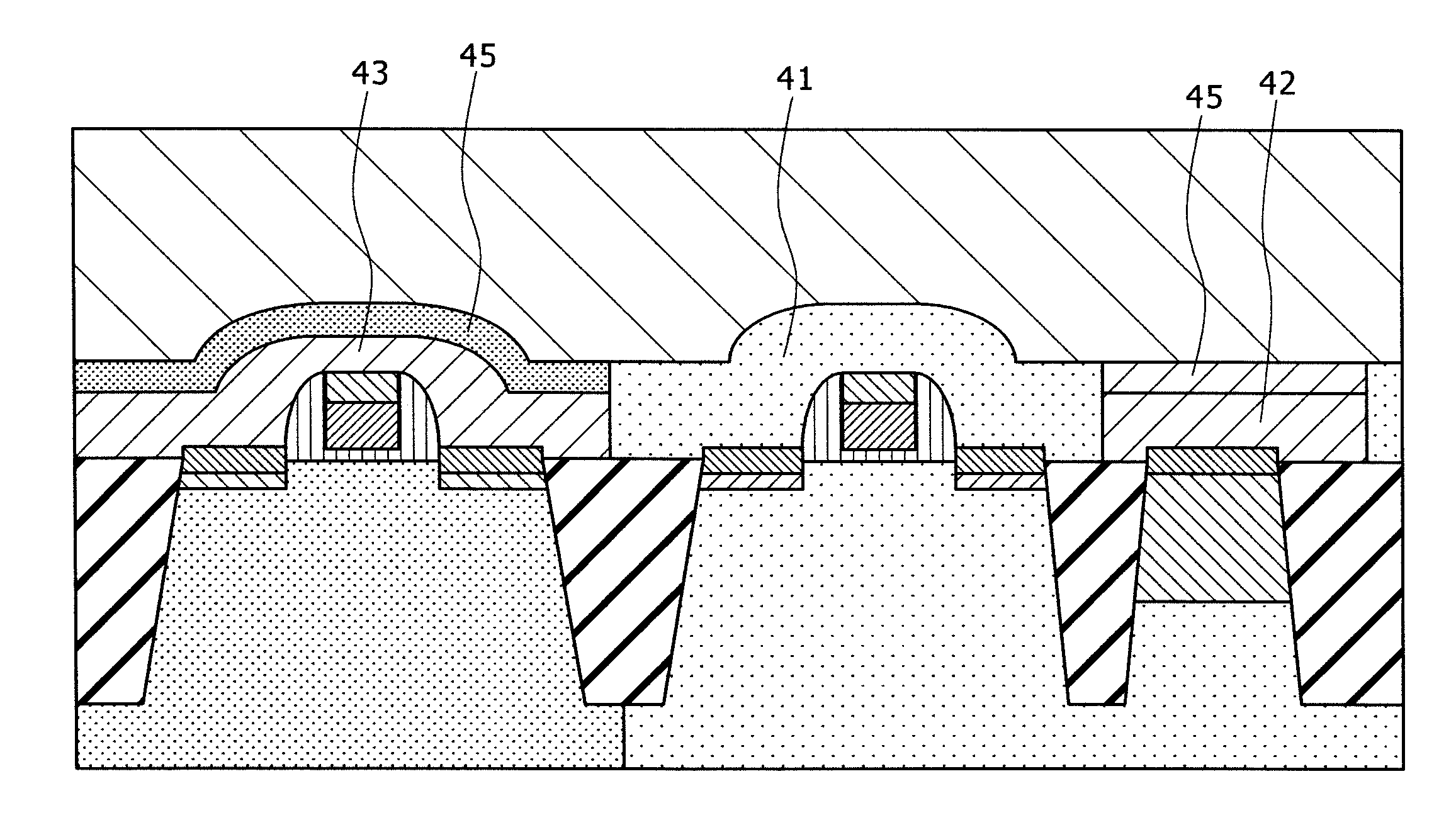
[0038]Furthermore, over the P-type field effec...

second embodiment

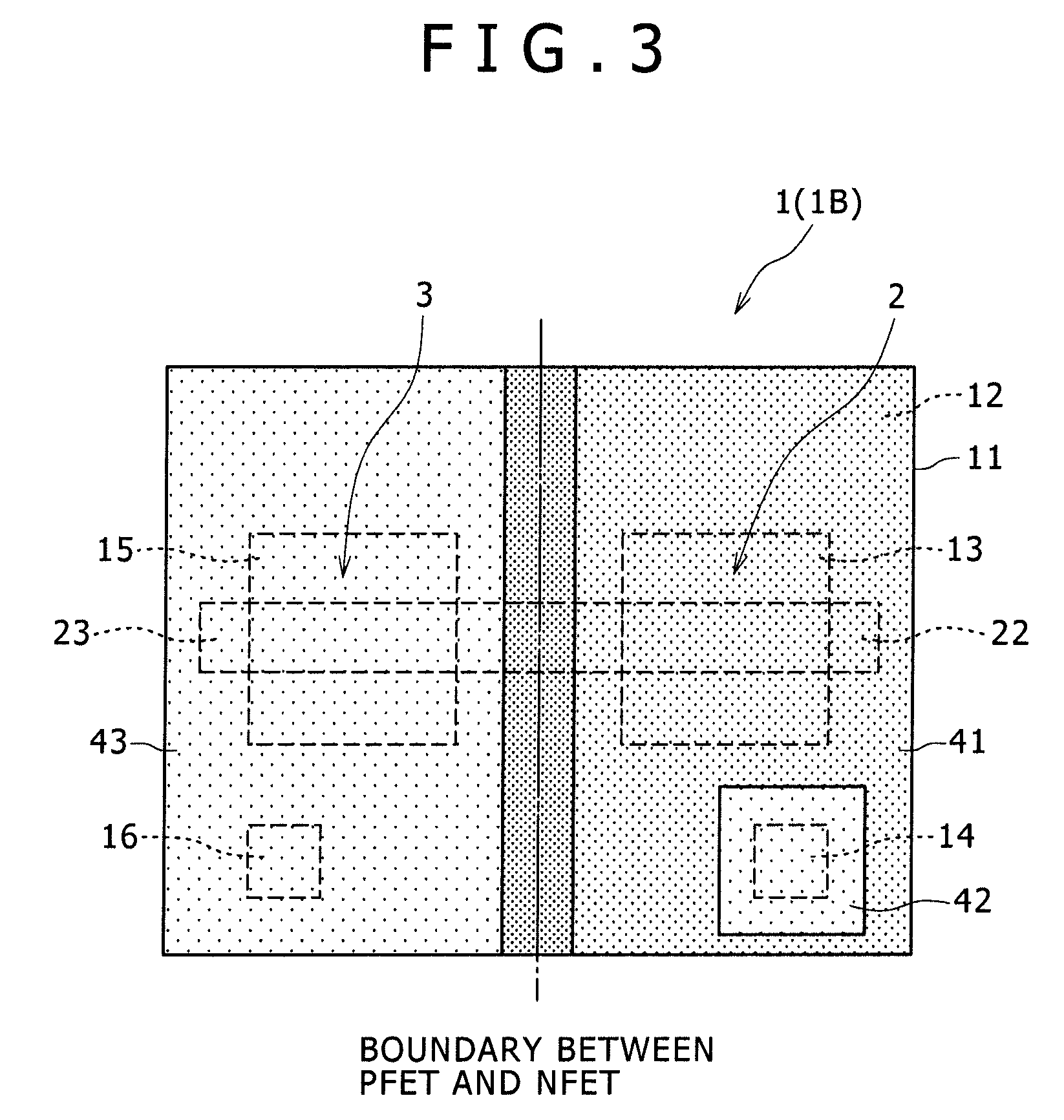
[0043]A semiconductor device according to one embodiment (second embodiment) of the present invention will be described below with reference to a layout plane view of FIG. 3.

[0044]As shown in FIG. 3, by an element isolation region 12 formed in a semiconductor substrate 11, a first element formation region 13 as the formation region of a P-type field effect transistor 2, an N-type substrate region 14 serving as a contact region, a second element formation region 15 as the formation region of an N-type field effect transistor 3, and a P-type substrate region 16 serving as a contact region are isolate from each other.

[0045]The P-type field effect transistor 2 is formed in the first element formation region 13. In the N-type substrate region 14, arsenic is ion-implanted to a deep position (e.g. to a position deeper than the source and drain regions of the transistor). On this N-type substrate region 14, a nickel silicide layer (not shown) is formed e.g. across the entire surface of the ...

third embodiment

[0051]A semiconductor device according to one embodiment (third embodiment) of the present invention will be described below with reference to layout plane views of FIGS. 4 and 5. FIGS. 4 and 5 show one example of application to a semiconductor device that serves as a NAND circuit.

[0052]As shown in FIG. 4, by an element isolation region 12 formed in a semiconductor substrate 11, a first element formation region 13 as the formation region of a P-type field effect transistor 2, an N-type substrate region 14 serving as a contact region, a second element formation region 15 as the formation region of an N-type field effect transistor 3, and a P-type substrate region 16 serving as a contact region are isolate from each other.

[0053]In the first element formation region 13, two P-type field effect transistors 2 are formed as one example. In the regions of the respective sources and drains in the first element formation region 13, e.g. plural contacts 31, contacts 32, and contacts 33 are fo...


PUM


Abstract

The present invention provides a semiconductor device includes: an element isolation region configured to be formed in a semiconductor substrate; a P-type field effect transistor configured to be formed in a first element formation region of the semiconductor substrate for which isolation by the element isolation region is carried out; an N-type substrate region configured to be formed in the semiconductor substrate for which isolation by the element isolation region is carried out, arsenic being ion-implanted into the N-type substrate region; a nickel silicide layer configured to be formed on the N-type substrate region; a first insulating film configured to cover the P-type field effect transistor and have compressive stress; and a second insulating film configured to cover the N-type substrate region and have tensile stress or compressive stress lower than the compressive stress of the first insulating film.

Description

CROSS REFERENCES TO RELATED APPLICATIONS[0001]The present invention contains subject matter related to Japanese Patent Application JP 2007-275882, filed in the Japan Patent Office on Oct. 24, 2007, the entire contents of which being incorporated herein by reference.BACKGROUND OF THE INVENTION[0002]1. Field of the Invention[0003]The present invention relates to a semiconductor device and a method for manufacturing the same.[0004]2. Description of Related Art[0005]In order to enhance the performance of semiconductor LSI devices, traditionally, the design scale is decreased to 0.7 times that of the previous-generation devices based on the Moore's scaling law, to thereby attempt improvement regarding the circuit processing speed, the power consumption, and so on. However, for LSI devices of the 45-nm-generation and the subsequent generations, it is becoming impossible to achieve enhanced performance through mere size shrinking, due to the influence of the abrupt deterioration of the sho...

Claims


Application Information

Patent Timeline
Patent Type & Authority Applications(United States)
IPC IPC(8): H01L47/00H01L21/76
CPCH01L21/823807H01L27/0207H01L29/7843H01L2924/0002H01L2924/00
Inventor YOKOYAMA, TAKASHI
Owner SONY CORP
Why Eureka
Try Eureka