

Semiconductor device
- Summary
- Abstract
- Description
- Claims
- Application Information
AI Technical Summary
Benefits of technology
Problems solved by technology
Method used
Image

Examples
embodiment 1
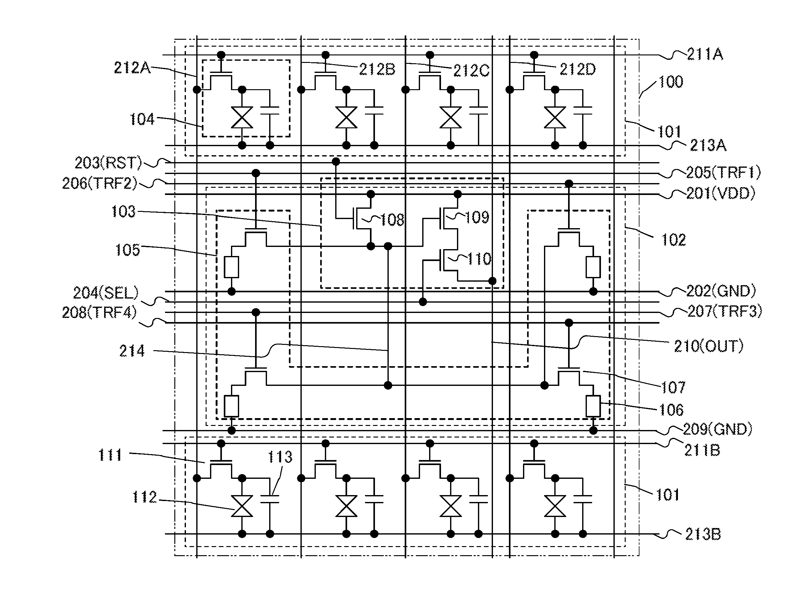
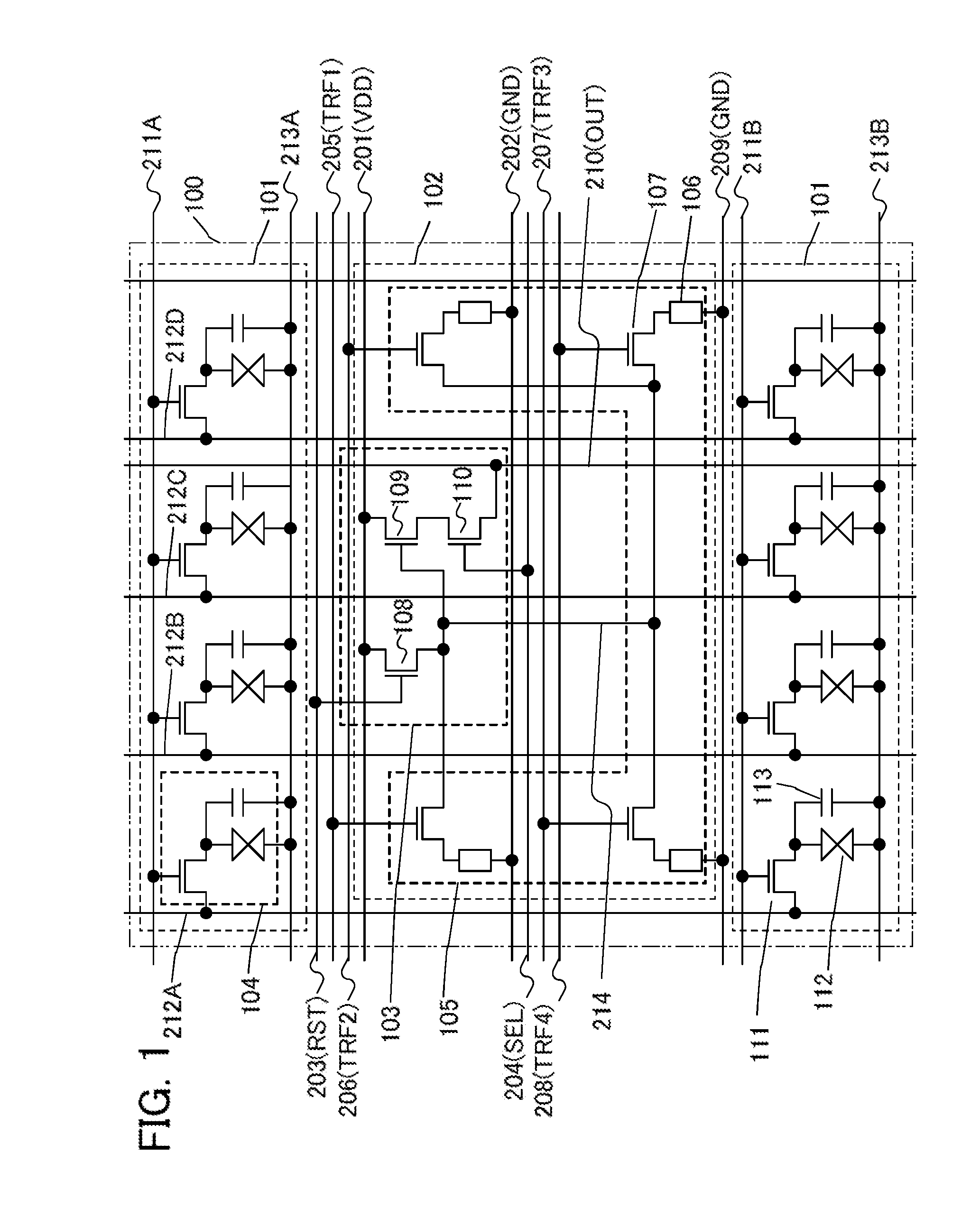
[0040]Described in this embodiment is a semiconductor device in which one amplifier circuit portion is shared by a plurality of unit pixels so as to reduce the area of a photosensor circuit corresponding to the unit pixel. The dead space in a display portion is reduced, resulting in an increase in the aperture ratio of the unit pixel.
[0041]FIG. 1 illustrates part of a display portion in the semiconductor device of one embodiment of the present invention. Note that FIG. 1 illustrates an example of the circuit configuration, and one embodiment of the present invention is not limited to this configuration.
[0042]A display portion 100 includes a pixel circuit 101 and a photosensor circuit 102. The pixel circuit 101 includes eight unit pixels 104. The photosensor circuit 102 includes an amplifier circuit portion 103 and a light-receiving portion 105.
[0043]Note that this embodiment shows an example in which the one amplifier circuit portion 103 is shared by the eight unit pixels 104; howev...
embodiment 2
[0090]Described in this embodiment is a case where the semiconductor device of one embodiment of the present invention includes a reflective liquid crystal display area.
[0091]An example of a method for manufacturing a reflective liquid crystal display device, which includes a non-single-crystal semiconductor layer in a light-receiving element and an oxide semiconductor layer in a transistor, will be described with reference to FIG. 4. An area from A to B in FIG. 4 is part of a unit pixel, and an area from C to D is part of a photosensor circuit. Note that the structure of the unit pixel and the photosensor circuit is not limited to this.
[0092]First, a conductive film is formed over a substrate 230, and then, a scan line 227, a capacitor wiring 224, a signal line 208, and a power source line 264 are formed using the conductive film. Although not illustrated, a selection line, an electrode line, a reset line, a ground line, and the like are also formed. In this embodiment, a glass sub...
embodiment 3
[0144]Described in this embodiment is a case where the semiconductor device of one embodiment of the present invention includes a light-transmitting liquid crystal display area. Note that in this embodiment, portions which are the same as those in Embodiment 2 are denoted by the same reference numerals, and description thereof will be omitted.
[0145]An example of a light-transmitting liquid crystal display device, which includes a non-single-crystal semiconductor layer in a light-receiving element and an oxide semiconductor layer in a transistor, will be described with reference to FIG. 5. An area from A to B in FIG. 5 is part of a unit pixel, and an area from C to D is part of a photosensor circuit. Note that the structure of the unit pixel and the photosensor circuit is not limited to this.
[0146]The insulating layer 241 of the semiconductor device in FIG. 5 is formed so as to have a flat surface without unevenness.
[0147]In the semiconductor device illustrated in FIG. 5, an electrod...
PUM
 Abstract
Description
Claims
Application Information