Method of manufacturing the trench power semiconductor structure

a manufacturing method and semiconductor technology, applied in the direction of semiconductor devices, basic electric elements, electrical equipment, etc., can solve the problems of high manufacturing cost and high cost of masking process, and achieve the effect of reducing high manufacturing cos

Inactive Publication Date: 2013-12-12
SUPER GROUP SEMICON
View PDF1 Cites 0 Cited by
  • Summary
  • Abstract
  • Description
  • Claims
  • Application Information

AI Technical Summary

Benefits of technology

[0007]Accordingly, the present invention provides a method of manufacturing the trench power semiconductor structure. First, the dielectric pattern layer is formed in the active region and the terminal region. Then, a first epitaxial layer is selectively formed on the base without being covered by the dielectric layer. Next, the dielectric pattern layer in the active region is removed, and the dielectric pattern layer in the terminal region is remained to act as the mask for forming the body and the source. Thus, one of the mask processes might be omitted to reduce the high manufacturing cost and the manufacturing error in the process of mask alignment.
[0008]According to the method of manufacturing the trench power semiconductor in present invention, only five masks are needed in the process from the base to the passivation layer, so as to reduce the manufacturing cost entirely and further promote the competition advantage in the price.

Problems solved by technology

The requirement of the design specification becomes stricter day by day, and thus it is a big challenge to the designer of the power converter device.
In the initial stage of element development, the cost of the masking process is very expensive.
Besides, the time wasting and the error in the process of manufacturing MOSFET might also increase the manufacturing cost.
Nowadays, in the semiconductor market, the competition advantage of the price is very important, and thus, searching for a simple manufacturing method to reduce the complication of the process and promote the competition advantage of the price without affecting the efficiency of the element is an important issue in this technical field.

Method used


Image

  • Method of manufacturing the trench power semiconductor structure
  • Method of manufacturing the trench power semiconductor structure
  • Method of manufacturing the trench power semiconductor structure

Examples


first embodiment

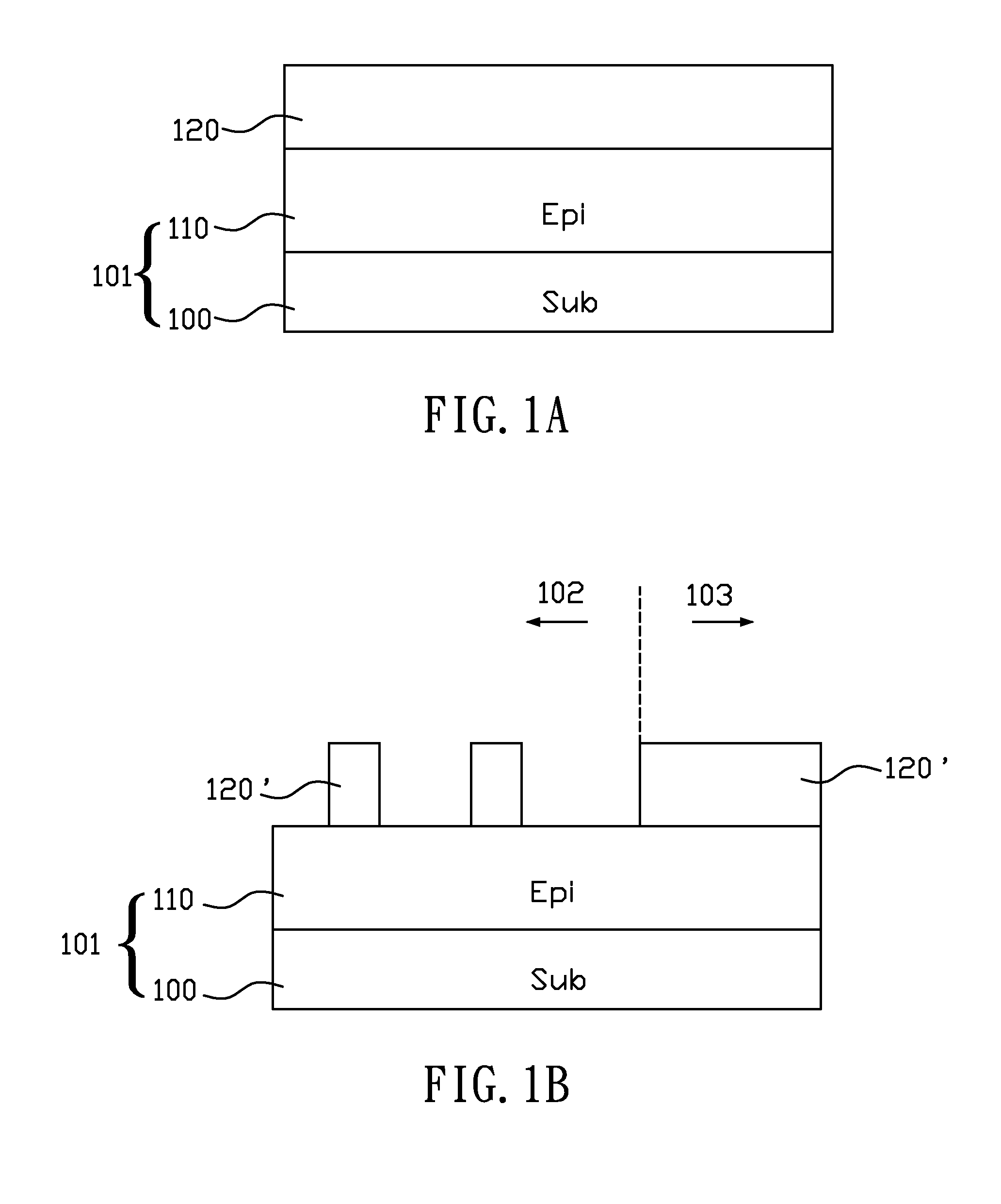
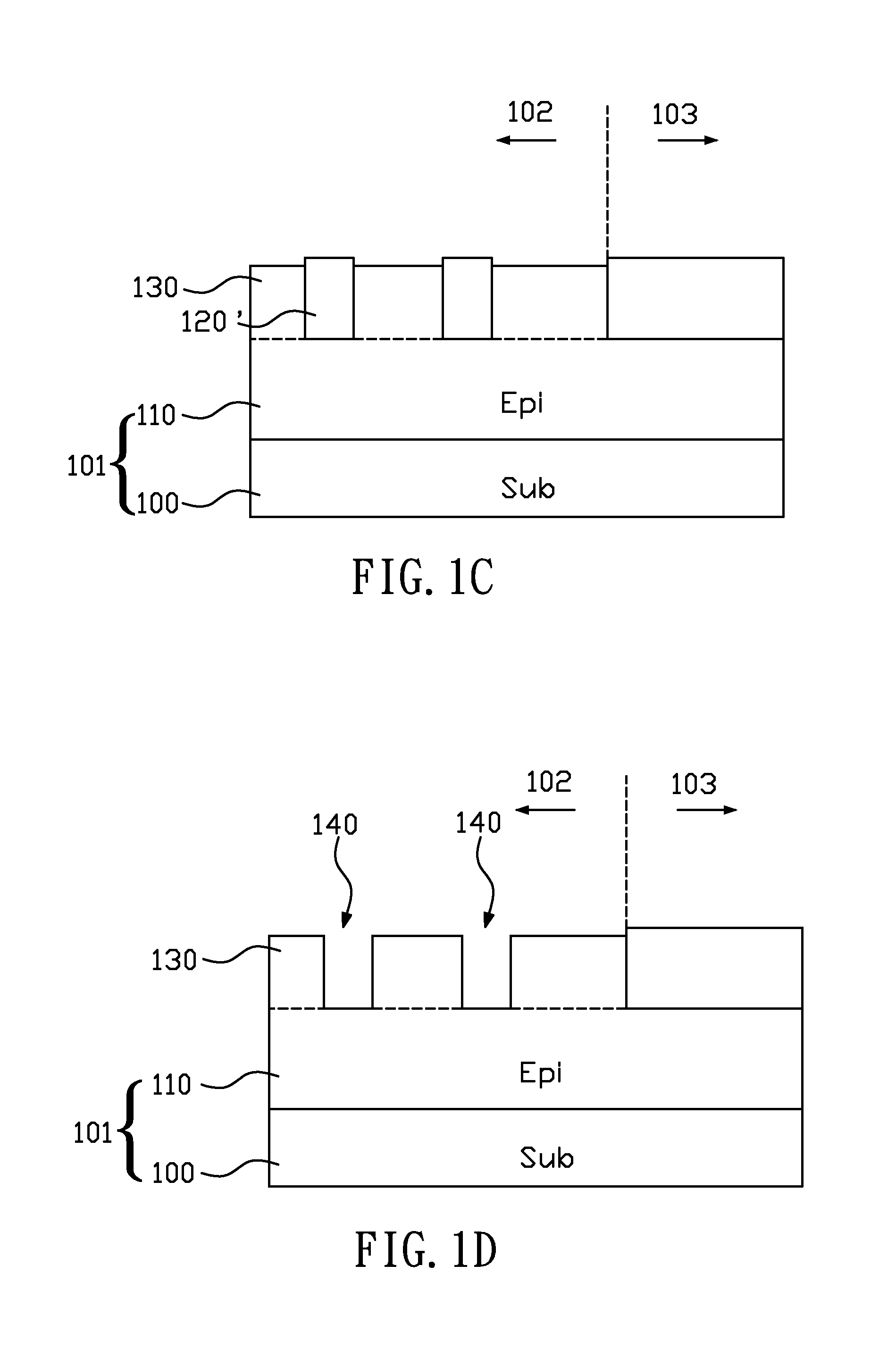
[0017]FIG. 1A to FIG. 1G illustrate the method of manufacturing the trench power semiconductor structure according to the first embodiment of present invention. As shown in the FIG. 1A, firstly, a base 101 is provided, which comprises a substrate 100 and an epitaxial layer 110. Then, a dielectric layer 120 is formed on the base 101. The dielectric layer 120 is deposited on the epitaxial layer 110, for example, but the present invention is not limited thereto. For example, the dielectric layer 120 can be form on the epitaxial layer 110 by using an oxidation manner. Next, the photolithography process is proceeded to form a dielectric pattern layer 120′ on the base 101, and thus to define an active region 102 and a terminal region 103 on the base 101. As shown in the FIG. 1B, only a portion of the epitaxial layer 110 in the active region 102 is covered by the dielectric pattern layer 120′, and all of the epitaxial layer 110 in the terminal region 103 is covered by the dielectric patter...

second embodiment

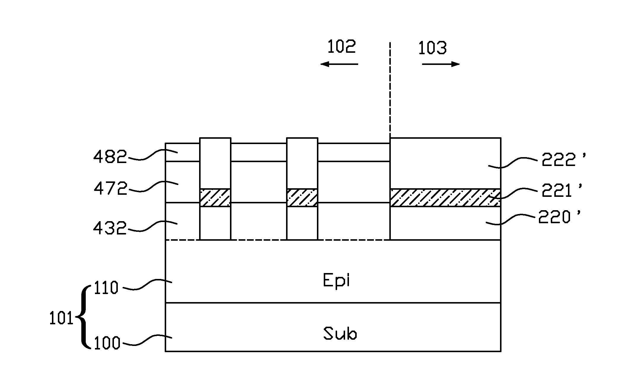
[0023]Furthermore, in order to obtain a lower gate-drain capacitance (Cgd), the bottom dielectric structure is formed under the gate trench according to the structure variation of the above-mentioned dielectric pattern layer 120′. The practical implementation is shown in FIG. 2A through FIG. 2E, which illustrate the method of manufacturing the trench power semiconductor structure according to the second embodiment of present invention.

[0024]As shown in the FIG. 2A, first of all, the epitaxial layer 110 is formed on the base 100. Then, a dielectric layer is formed on the base 100, wherein the dielectric layer comprises a bottom dielectric layer 220, an isolating layer 221 and a shielding layer 222. The silicon nitride would be selected as the material of the above-mentioned isolating layer 221 and the present invention is not limited thereto. The material of the isolating layer 221 should be different from that of the bottom dielectric layer 220 and the shielding layer 222. Besides, ...

third embodiment

[0028]FIG. 3A through FIG. 3C illustrate the method of manufacturing the trench power semiconductor structure according to the third embodiment of present invention. This embodiment is different from the first embodiment in which the source and the body are formed after the gate dielectric layer. Instead, the source and the body are formed before the gate dielectric layer in this embodiment. As shown in the FIG. 3A, which is the step right after the first epitaxial layer 130 formed in the FIG. 1C of the first embodiment, by utilizing the dielectric pattern layer 120′ in the active region 102 and in the terminal region 103 as the mask, and by using the ion implantation manner, a body 370 in the first epitaxial layer 130 is formed. After that, a source 380 is formed on the upper portion of the body 370.

[0029]Next, as shown in the FIG. 3B, the dielectric pattern layer 120′ in the active region 102 is removed to form a gate trench 340 on the epitaxial layer 110. Then, the bottom of the ...


PUM


Abstract

A method of manufacturing a trench power semiconductor structure is provided. The method comprising the steps of: providing a base, forming a dielectric pattern layer on the base to define an active region and a terminal region, wherein a portion of the base in the active region and the terminal region is covered by the dielectric pattern layer; selectively forming a first epitaxial layer on the base without being covered by the dielectric pattern layer; removing the dielectric pattern layer in the active region to form a gate trench on the base, and forming a gate dielectric layer on the first epitaxial layer and on the inner surface of the gate trench; forming the gate structure in the gate trench; utilizing the dielectric pattern layer to forming a body on or in the first epitaxial layer; and forming a source on the upper portion of the body.

Description

BACKGROUND[0001]1. Technical Field[0002]The invention relates to a method of manufacturing power semiconductor structure, and in particular the method of manufacturing the trench power semiconductor structure.[0003]2. Description of Related Art[0004]With the higher requirement of energy conservation, the higher energy conversion efficiency is needed. The requirement of the design specification becomes stricter day by day, and thus it is a big challenge to the designer of the power converter device. In order to meet this requirement, the power converter device in the high converter efficiency becomes more and more important, wherein the power metal-oxide-semiconductor field effect transistor (Power MOSFET) is one of the most widely used in the power converter devices.[0005]In the traditional planar MOSFET, the current is flowing along with the base surface. On the other hand, in the trench MOSFET, the gate is set in the trench, and the channel position of the MOSFET is changed, so as...

Claims


Application Information

Patent Timeline
Patent Type & Authority Applications(United States)
IPC IPC(8): H01L21/336
CPCH01L29/42368H01L29/66734H01L29/7811H01L29/7813
Inventor HSU, HSIU-WEN
Owner SUPER GROUP SEMICON
Why Eureka
Try Eureka