Dicing die bond film and method of manufacturing semiconductor device

a technology of die bonding film and semiconductor chip, which is applied in the direction of semiconductor/solid-state device details, thin material processing, semiconductor devices, etc., can solve the problems of poor reliability of bonding a semiconductor chip, low bonding strength between the electrode member and the semiconductor chip, and poor characteristic, so as to reduce friction with the push-up jig and suitably reduce the effect of friction

Inactive Publication Date: 2013-12-12
NITTO DENKO CORP
View PDF13 Cites 38 Cited by
  • Summary
  • Abstract
  • Description
  • Claims
  • Application Information

AI Technical Summary

Benefits of technology

[0027]In the above-described configuration, the dynamic friction coefficient of the contact part of the dicing film is preferably 0 to 0.02. When the dynamic friction coefficient of the contact part of the dicing film is 0.2 or less, the friction with the push-up jig can be decreased when the tensile force is applied, and the die bond film can be broken in a normal manner.
[0028]In the above-described configurati...

Problems solved by technology

As a result, the thickness of the formed paste-form adhesive layer becomes uneven so that the reliability in strength of bonding a semiconductor chip is poor.
In other words, if the amount of the paste-form adhesive coated on an electrode member is insufficient, the bonding strength between the electrode member and a semiconductor chip becomes low so that in a subsequent wire bonding step, the semiconductor chip is peeled.
On the other hand, if the amount of the coated paste-form adhesive is too large, this adhesive flows out to stretch over the semiconductor chip so that the characteristic becomes poor.
Thus, the yield or the reliability lowers.
Such problems about the adhesion treatment become particularly remarkable with an increase in the size of semiconductor chips.
Thus, the workability or the productivity is deteriorated.
In this method, however, it is difficult to make th...

Method used


Image

  • Dicing die bond film and method of manufacturing semiconductor device
  • Dicing die bond film and method of manufacturing semiconductor device
  • Dicing die bond film and method of manufacturing semiconductor device

Examples


Embodiment Construction

(Dicing Die Bond Film)

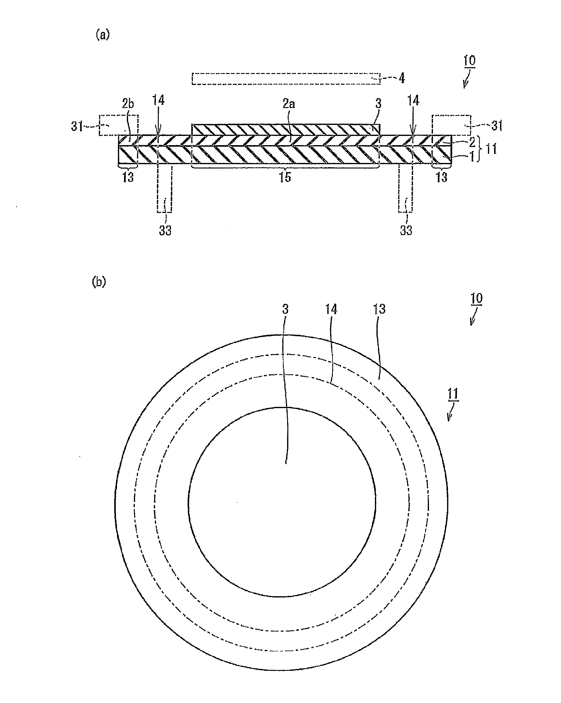
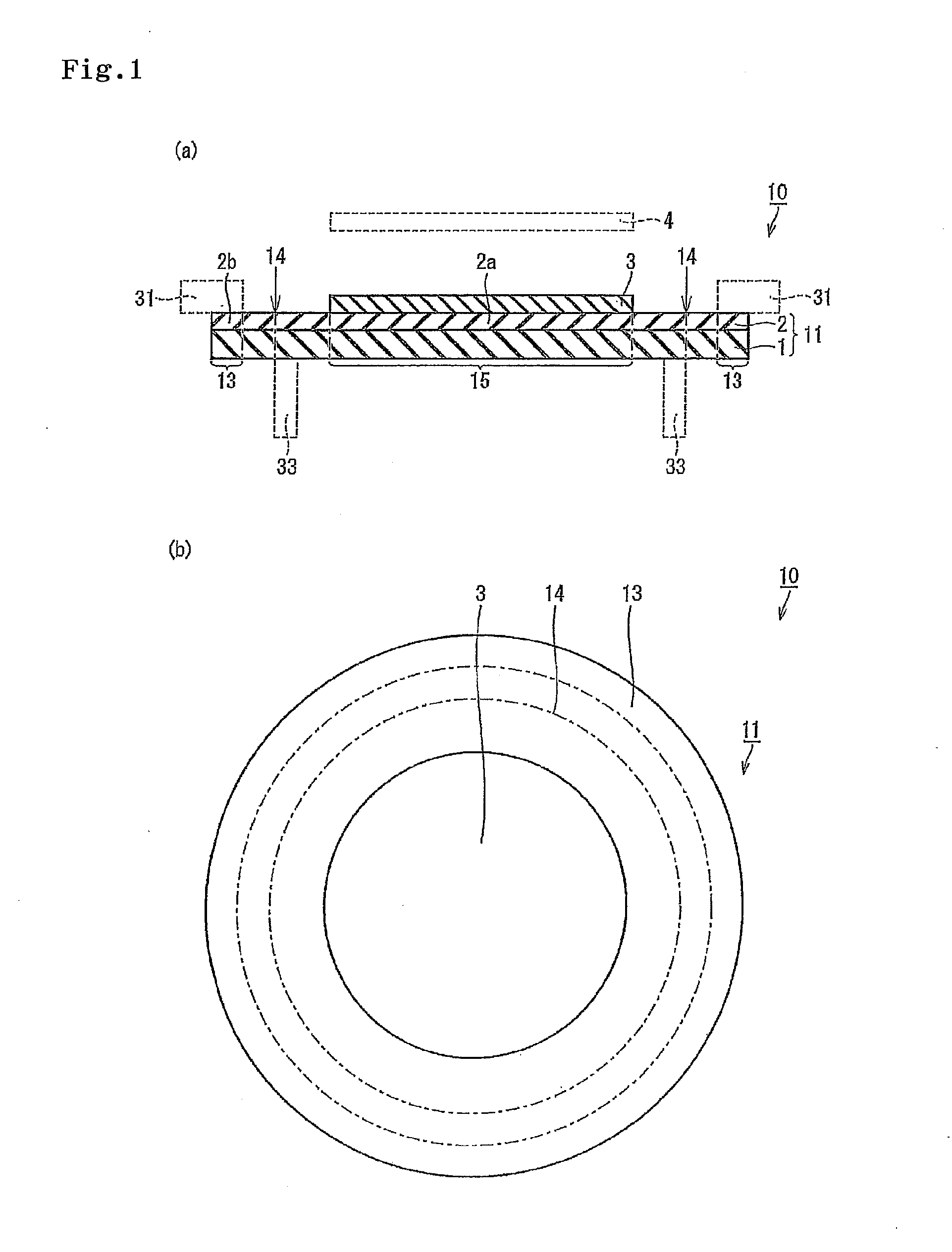
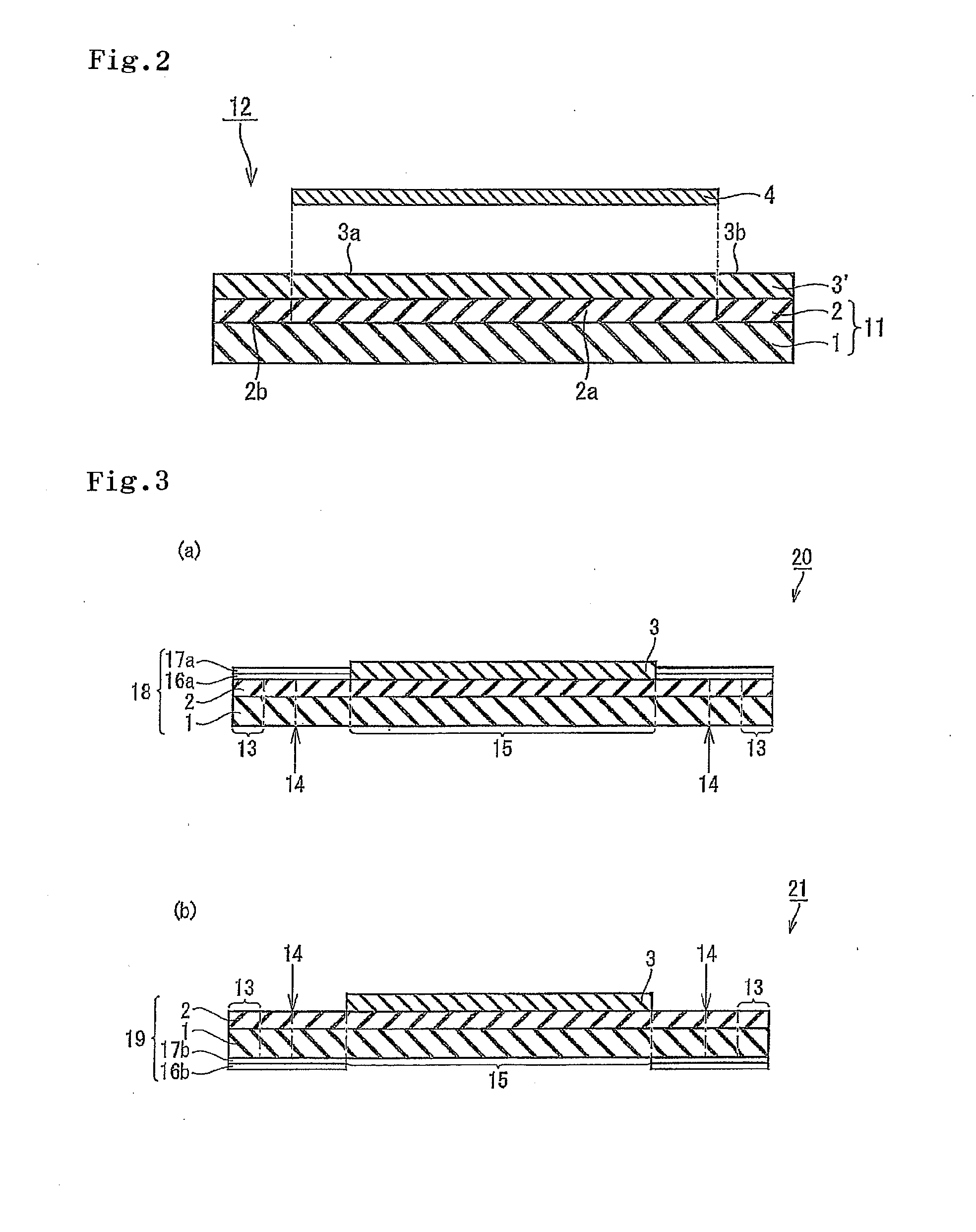
[0056]The dicing die bond film according to the present embodiment is explained below. FIG. 1(a) is a cross-sectional schematic diagram showing the dicing die bond film according to one embodiment of the present invention, and FIG. 1(b) is its planar drawing. FIG. 2 is a cross-sectional schematic diagram showing the dicing die bond film according to another embodiment of the present invention.

[0057]A dicing die bond film 10 has a configuration in which a die bond film 3 is laminated on a dicing film 11. A pressure-sensitive adhesive layer 2 is laminated on a base 1 to configure the dicing film 11, and the die bond film 3 is provided on the pressure-sensitive adhesive layer 2. The die bond film 3 is formed only on a part 2a corresponding to the semiconductor wafer bonding part of the pressure-sensitive adhesive layer 2. In the present invention, a configuration may be adopted in which a die bond film 3′ is formed on the entire surface of the dicing film 11 as sh...


PUM


Abstract

The present invention provides a dicing die bond film in which yielding and breaking of the dicing film are prevented and in which the die bond film can be suitably broken with a tensile force. In the dicing die bond film of the present invention, the tensile strength of the contact part in which the outer circumference of the push-up jig contacts the dicing film at 25° C. is 15 N or more and 80 N or less and the yield point elongation is 80% or more, the tensile strength of the wafer bonding part of the dicing film at 25° C. is 10 N or more and 70 N or less and the yield point elongation is 30% or more, [(the tensile strength of the contact part)−(the tensile strength of the wafer bonding part)] is 0 N or more and 60 N or less, and the breaking elongation rate of the die bond film at 25° C. is more than 40% and 500% or less.

Description

TECHNICAL FIELD[0001]The present invention relates to a dicing die bond film in which a die bond film and a dicing film are laminated. The present invention also relates to a method of manufacturing a semiconductor device using the dicing die bond film.BACKGROUND ART[0002]Conventionally, silver paste has been used to bond a semiconductor chip to a lead frame or an electrode member in the step of producing a semiconductor device. The treatment for the sticking is conducted by coating a paste-form adhesive on a die pad of a lead frame, or the like, mounting a semiconductor chip on the die pad, and then setting the paste-form adhesive layer.[0003]However, about the paste-form adhesive, the amount of the coated adhesive, the shape of the coated adhesive, and on the like are largely varied in accordance with the viscosity behavior thereof, a deterioration thereof, and on the like. As a result, the thickness of the formed paste-form adhesive layer becomes uneven so that the reliability in...

Claims


Application Information

Patent Timeline
IPC IPC(8): H01L21/78
CPCH01L21/78H01L21/6836H01L2221/68336H01L2221/68377H01L2224/48091H01L2224/73265H01L2224/83191H01L24/27H01L2224/45144H01L2224/45147H01L2924/10253H01L2224/45124H01L2221/6834H01L2221/68381H01L2924/01015H01L2924/01047H01L23/3121H01L2924/3025H01L24/45H01L24/48H01L2224/85207H01L2924/15747H01L2924/15788H01L2924/181H01L2924/12042Y10T428/24331H01L2924/00014H01L2924/00H01L2924/00012H01L21/30H01L21/52
Inventor TANAKA, SHUMPEIMATSUMURA, TAKESHI
Owner NITTO DENKO CORP
Why Eureka
Try Eureka