Monolithic compound semiconductor structure

a semiconductor structure and compound technology, applied in semiconductor devices, diodes, transistors, etc., can solve the problems of limiting the protection level of esd, device degradation or damage, etc., and achieve the effect of improving esd performance, reducing the surface area of the chip, and increasing product competitiveness

Active Publication Date: 2013-12-19
WIN SEMICON
View PDF12 Cites 3 Cited by
  • Summary
  • Abstract
  • Description
  • Claims
  • Application Information

AI Technical Summary

Benefits of technology

[0006]The main object of the present invention is to provide a monolithic compound semiconductor structure, in which a n-type etching-stop layer and a p-type insertion layer are included in a BiFET structure, so that the epitaxial structure of an FET, an HBT, and a thyristor can be integrated in a compound semiconductor monolithic chip. The thyristor therein can be used in an ESD system. The surface area of a chip herewith is significantly reduced comparing with a conventional ESD system using diodes. Furthermore, the ESD performance can be improved, and thus the product competitiveness can be increased.

Problems solved by technology

The discharging process may produce a current of several amps within a few nanoseconds, leading to device degradation or damage.
Besides, the turn-on voltage of a diode is small, which in turn limits the ESD protection level.

Method used


Image

  • Monolithic compound semiconductor structure
  • Monolithic compound semiconductor structure
  • Monolithic compound semiconductor structure

Examples


Embodiment Construction

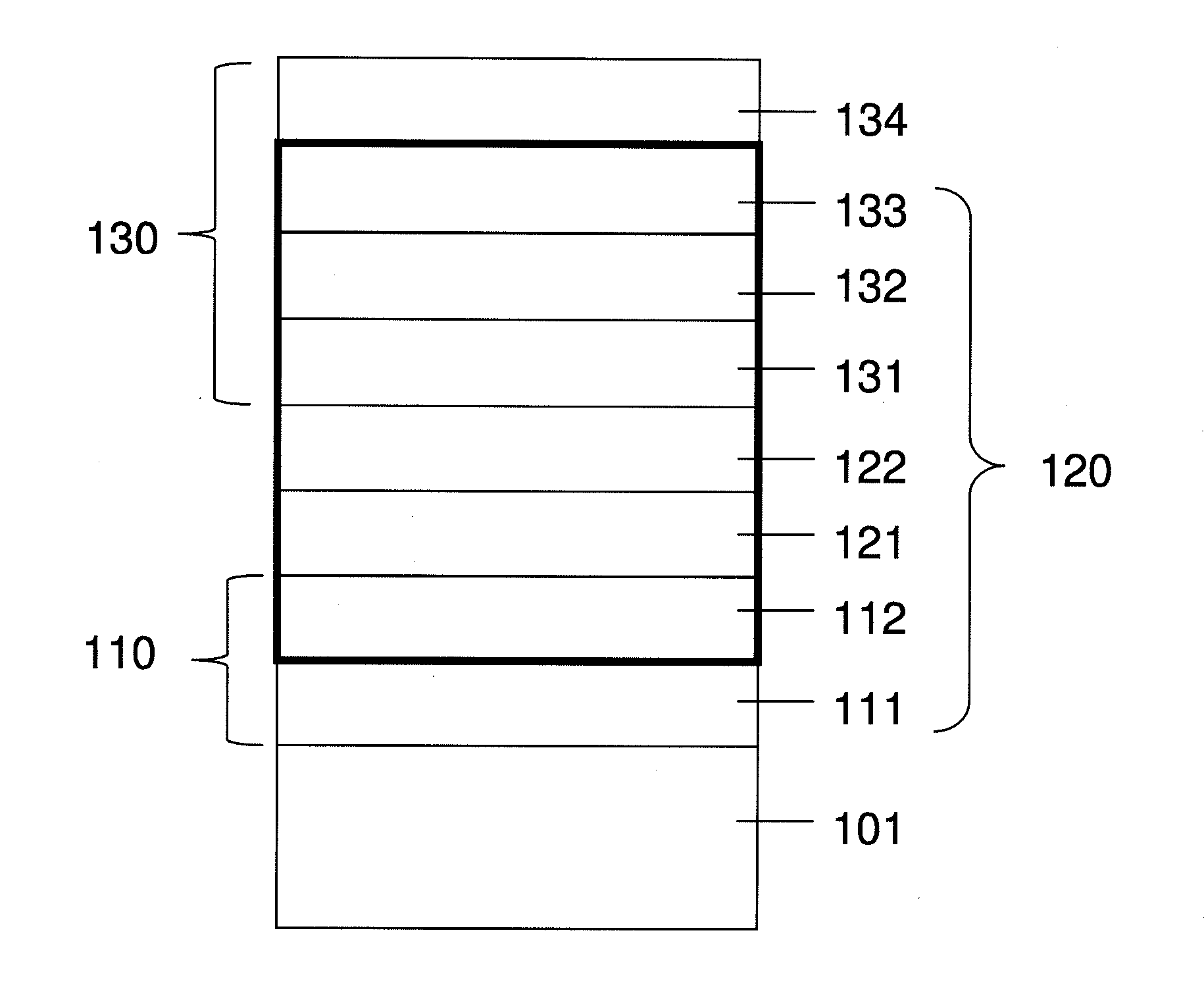
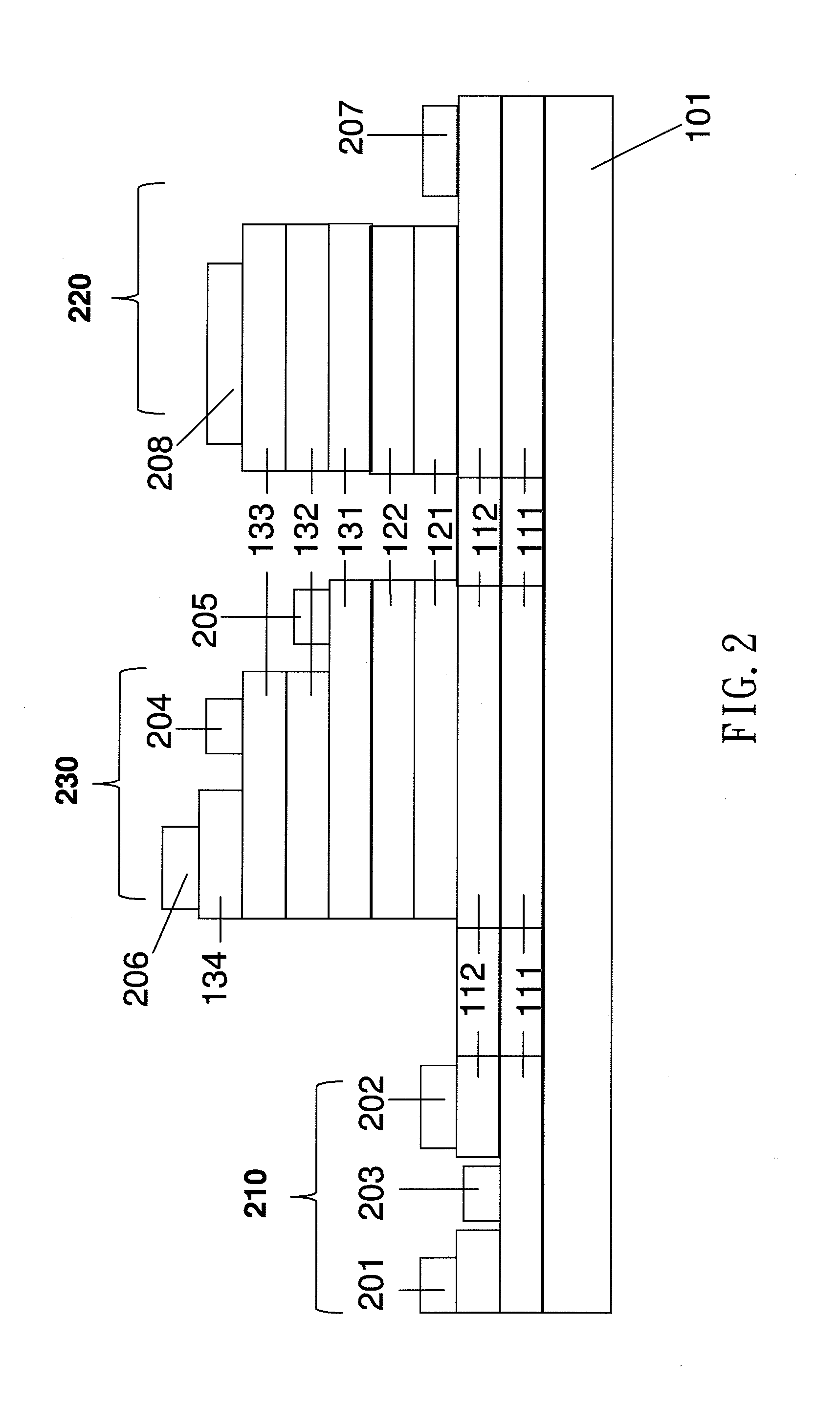
[0022]The monolithic compound semiconductor structure integrating the epitaxial structure of an FET, an HBT, and a thyristor provided by the present invention is shown schematically in FIG. 1. The structure comprises a substrate 101, an FET epitaxial structure 110, an n-type etching-stop layer 121, a p-type insertion layer 122, and an HBT epitaxial structure 130. The substrate 101 is made of a semi-insulating semiconductor material such as GaAs or InP, and the preferred material is GaAs. The FET epitaxial structure 110 is formed on the substrate 101. It comprises a channel layer 111, and an n-type doped layer 112 formed on the channel layer 111. The structure can be used to form an n-type FET. The n-type etching-stop layer 121 is formed on the FET epitaxial structure 110. The p-type insertion layer 122 is formed on the n-type etching-stop layer 121. The HBT epitaxial structure 130 from bottom to top sequentially comprises a sub-collector layer 131, a collector layer 132, a base laye...


PUM


Abstract

A monolithic compound semiconductor structure is disclosed. The monolithic compound semiconductor structure comprises a substrate, an n-type FET epitaxial structure, an n-type etching-stop layer, a p-type insertion layer, and an npn HBT epitaxial structure, and it can be used to form an FET, an HBT, or a thyristor.

Description

FIELD OF THE INVENTION[0001]The present invention relates to a monolithic compound semiconductor structure, and in particular, to a monolithic compound semiconductor structure integrating a heterojunction bipolar transistor (HBT), a field effect transistor (FET), and a thyristor for applications in electrostatic discharge (ESD) protection circuits.BACKGROUND OF THE INVENTION[0002]When a human body touches an integrated circuit, the accumulated electrostatic charges pass from the human body to the integrated circuit through the pins, and then the integrated circuit is discharged through the ground contact. The discharging process may produce a current of several amps within a few nanoseconds, leading to device degradation or damage. Therefore it is necessary to design an ESD protection system for the devices in an integrated circuit to sustain ESD events.[0003]In monolithic compound semiconductor structures, ESD protection circuits are usually composed of p-n junction diodes or Schot...

Claims


Application Information

Patent Timeline
Patent Type & Authority Applications(United States)
IPC IPC(8): H01L29/74
CPCH01L21/8252H01L27/0605H01L27/0623H01L29/205H01L29/7371H01L29/87
Inventor LIN, CHENG-KUOLI, SZU-JUSYU, RONG-HAOTSAI, SHU-HSIAO
Owner WIN SEMICON
Why Eureka
Try Eureka