Hybrid integrated component and method for the manufacture thereof

a technology of integrated components and manufacturing methods, applied in the field of hybrid integrated components, can solve the problems of comparatively small mounting surfaces, less and less space available for individual components, and manufacturing costs of terminal equipment, and achieve the effects of small component footprint, limited compatibility, and easy integration

Active Publication Date: 2013-12-19
ROBERT BOSCH GMBH
View PDF26 Cites 42 Cited by
  • Summary
  • Abstract
  • Description
  • Claims
  • Application Information

AI Technical Summary

Benefits of technology

[0009]It has been found according to the present invention that the circuit functions of the ASIC element do not have to be restricted within the scope of the known component concept to signal processing for the MEMS element, but rather the ASIC element may additionally be equipped with an independent sensor function. This sensor function is implemented within the scope of the preprocessing of the ASIC element or substrate and must therefore only have limited compatibility with respect to processing with the micromechanical processing of the MEMS substrate and the APT (assembly and packaging technology) of the component. The present invention utilizes the fact that a magnetic sensor system may be implemented very well in a layered structure. The deposition and structuring processes required for this purpose may be integrated easily into the process sequence for manufacturing a CMOS back-end stack on the ASIC substrate.
[0010]The component concept under discussion here, which is expanded according to the present invention, is particularly well-suited for equipping sensors which operate in a contactless way, for example, inertial sensors, with an additional compass function. In particular, three-axis accele

Problems solved by technology

Therefore, less and less space is available for the individual components on the application printed circuit boards.
In addition, the known components require a comparatively small mounting surface because of the stacked construction, which has a favorable effect on the manufacturing costs of the terminal equipm

Method used


Image

  • Hybrid integrated component and method for the manufacture thereof
  • Hybrid integrated component and method for the manufacture thereof
  • Hybrid integrated component and method for the manufacture thereof

Examples


Embodiment Construction

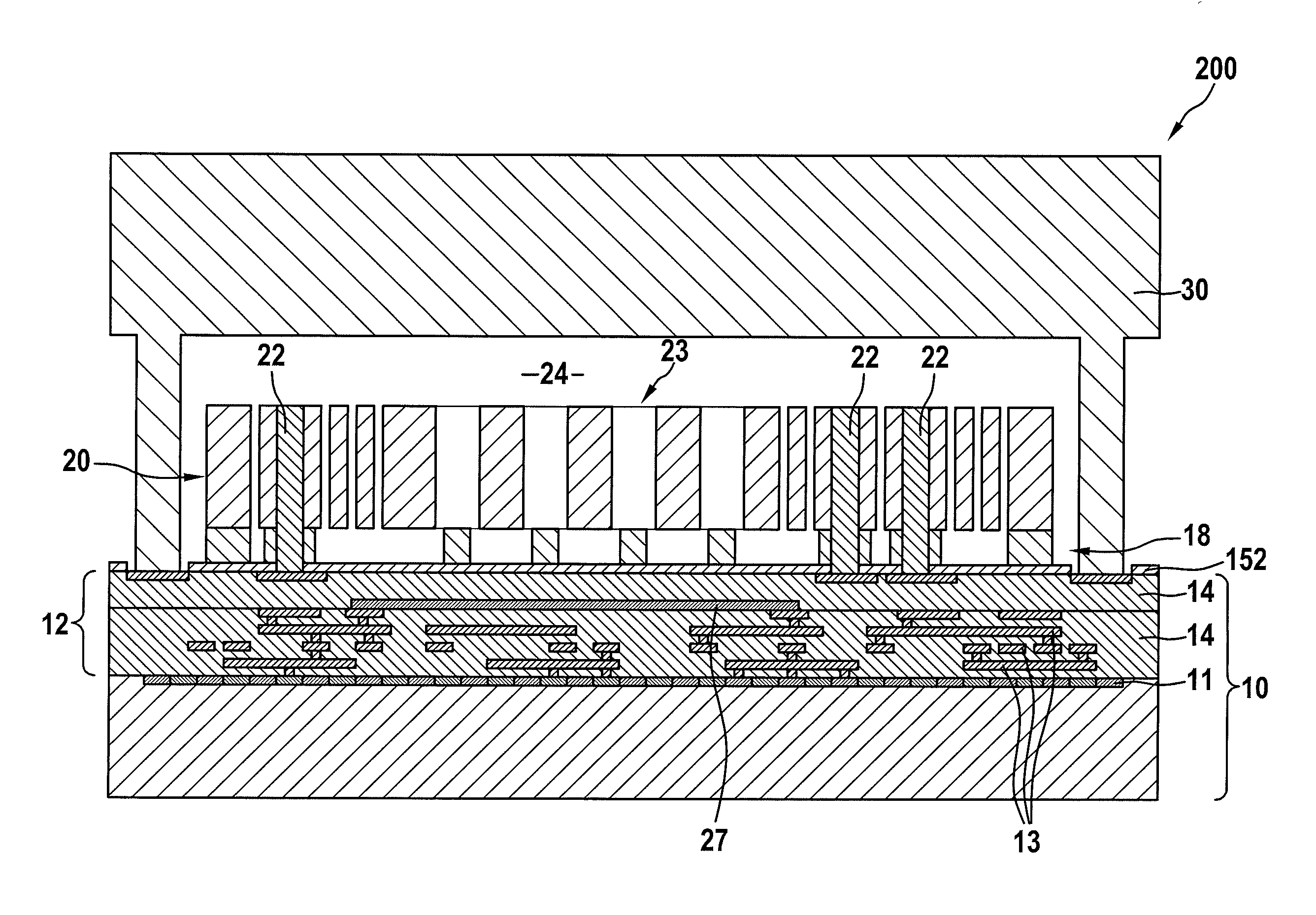
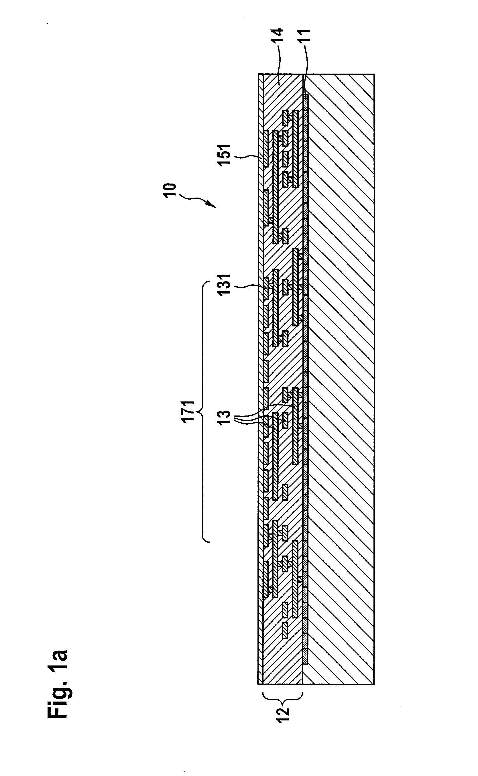
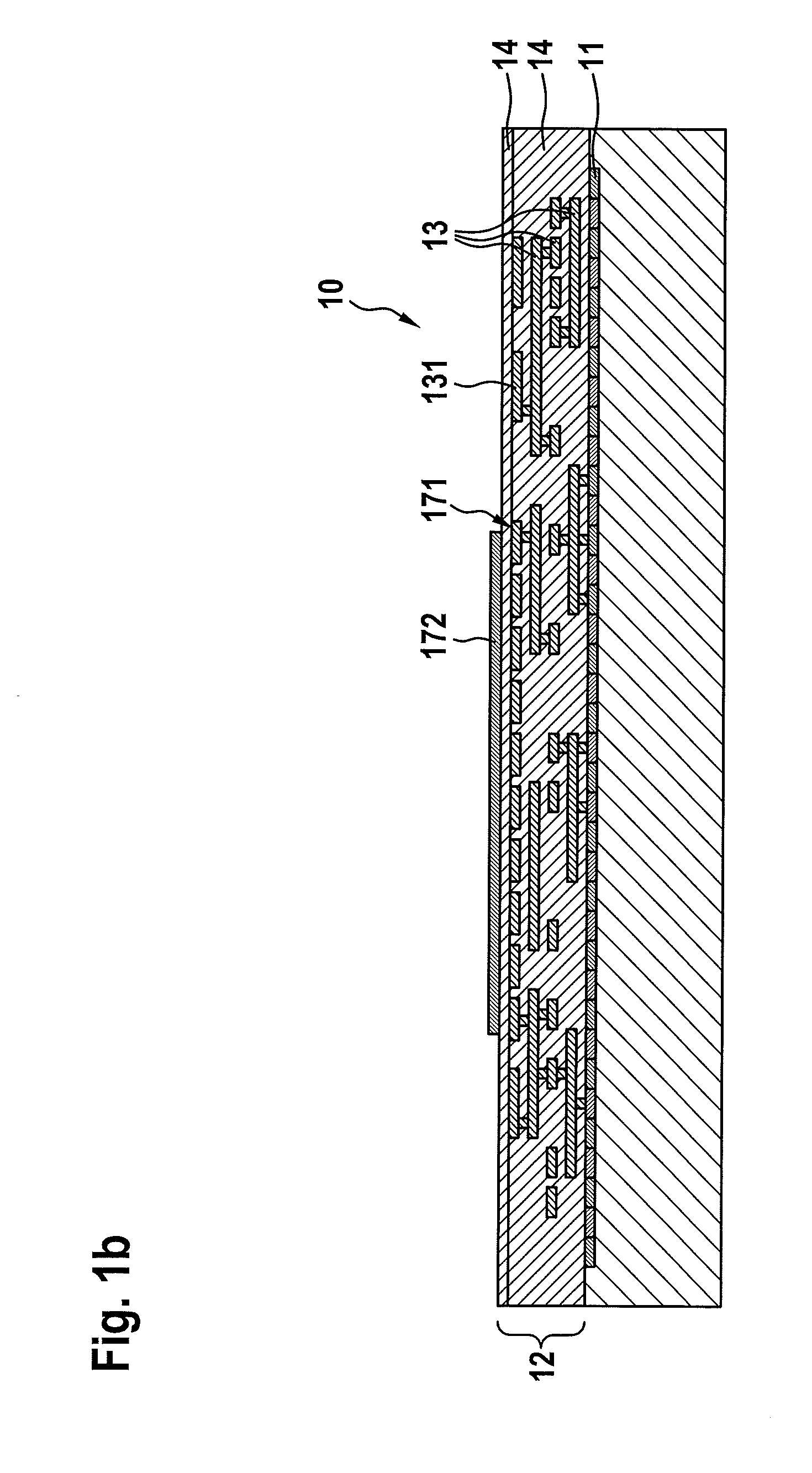
[0023]In the case of the two method variants, which are described hereafter in conjunction with FIGS. 1a through 1g and 3a through 3d, for manufacturing a hybrid integrated component including an MEMS element, a cap for the micromechanical structure of the MEMS element, and an ASIC element, the ASIC substrate is processed independently from the remaining component parts. Circuit elements 11 are integrated into ASIC substrate 10 in a CMOS process. These circuit elements 11 are advantageously at least parts of a signal processing and analysis circuit for the MEMS sensor function of the component to be manufactured. However, MEMS-independent circuit functions may also be integrated into ASIC substrate 10 within the scope of the CMOS processing. For the internal component electrical wiring of circuit elements 11, a CMOS back-end stack 12 is then produced on the processed surface of ASIC substrate 10. This is a layered structure having multiple circuit levels in the form of structured me...


PUM

PropertyMeasurementUnit
Thicknessaaaaaaaaaa
Structureaaaaaaaaaa
Areaaaaaaaaaaa

Abstract

An expansion of the functional scope of a hybrid integrated component including an MEMS element, a cap for the micromechanical structure of the MEMS element, and an ASIC element having circuit components is provided. In this component, the circuit components of the ASIC element interact with the micromechanical structure of the MEMS element. The MEMS element is mounted on the ASIC element in such a way that the micromechanical structure of the MEMS element is situated in a cavity between the cap and the ASIC element. The ASIC element is additionally equipped with the circuit components of a magnetic sensor system. These circuit components are produced in or on the CMOS back-end stack of the ASIC element. The magnetic sensor system may thus be implemented without enlarging the chip area.

Description

FIELD OF THE INVENTION[0001]The present invention relates to a hybrid integrated component including an MEMS (micro-electromechanical system) element, a cap for the micromechanical structure of the MEMS element, and an ASIC (application-specific integrated circuit) element having circuit components, which interact with the micromechanical structure of the MEMS element. The MEMS element is mounted on the ASIC element, so that the micromechanical structure of the MEMS element is situated in a cavity between the cap and the ASIC element. Furthermore, the present invention relates to methods for manufacturing such a hybrid integrated component.BACKGROUND INFORMATION[0002]Components having MEMS elements have been manufactured in mass production for many years for greatly varying applications, for example, in the field of automotive technology and consumer electronics. The miniaturization of the components is increasingly gaining significance. On the one hand, the miniaturization substant...

Claims


Application Information

Patent Timeline
IPC IPC(8): B81B3/00B81C1/00
CPCB81B3/0018B81C1/00261B81C2203/0771B81C1/00238B81C1/00246B81C2203/0735B81C2203/0785
Inventor CLASSEN, JOHANNESFARBER, PAUL
Owner ROBERT BOSCH GMBH
Why Eureka
Try Eureka