

Heat treatment method and heat treatment apparatus for heating substrate by irradiating substrate with light
a heat treatment method and heat treatment technology, applied in the direction of lighting and heating apparatus, drying machines, drying, etc., can solve the problems of increasing the leakage current, lowering device characteristics, and the interface between the deposited the underlying silicon dioxide film, so as to improve the interface characteristics and promote the crystallization of the high dielectric constant film
- Summary
- Abstract
- Description
- Claims
- Application Information
AI Technical Summary
Benefits of technology
Problems solved by technology
Method used
Image

Examples
Embodiment Construction
[0029]A preferred embodiment according to the present invention will now be described in detail with reference to the drawings.
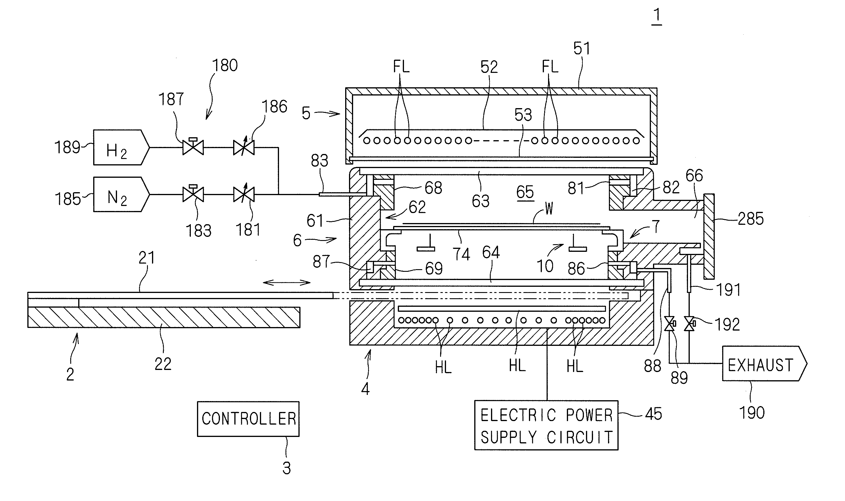
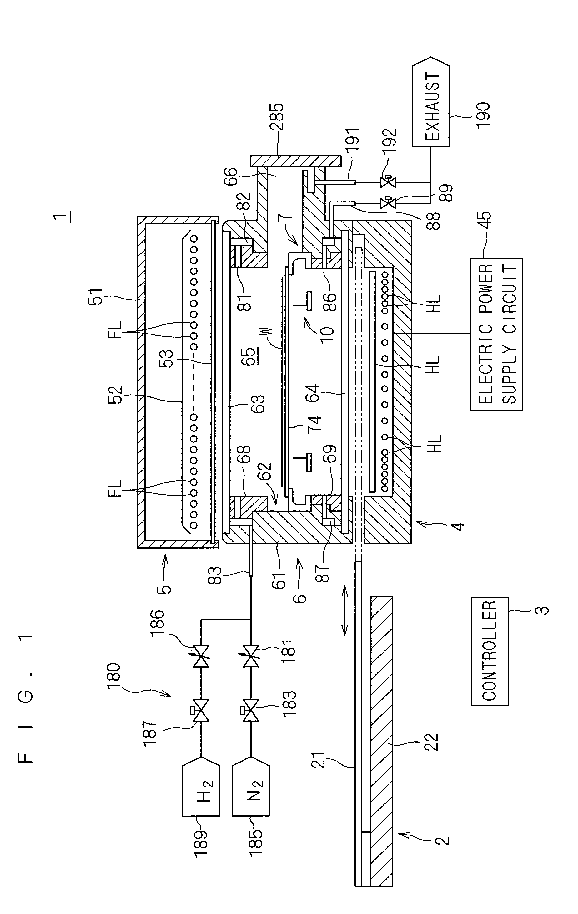
[0030]FIG. 1 is a longitudinal sectional view showing a configuration of a heat treatment apparatus 1 according to the present invention. The heat treatment apparatus 1 according to the present preferred embodiment is a flash lamp annealer for irradiating a disk-shaped semiconductor wafer W having a diameter of 300 mm and serving as a substrate with a flash of light to heat the semiconductor wafer W. A gate of a high dielectric constant film is formed on a semiconductor wafer W prior to the transport into the heat treatment apparatus 1, and the heat treatment apparatus 1 performs a heating treatment on the semiconductor wafer W to thereby promote the crystallization of the high dielectric constant film, which will be described in detail later.
[0031]The heat treatment apparatus 1 includes a chamber 6 for receiving a semiconductor wafer W therein, a flash heat...
PUM
 Abstract
Description
Claims
Application Information