
Radiological image detection apparatus and method of manufacturing the same

a technology of radiological image and detection apparatus, which is applied in the direction of radiation intensity measurement, instruments, x/gamma/cosmic radiation measurement, etc., can solve the problems of not disclosing the method of reducing ghosts and ghost generation, so as to reduce ghosts and improve sensitivity

Inactive Publication Date: 2014-01-02
FUJIFILM CORP
View PDF11 Cites 10 Cited by
  • Summary
  • Abstract
  • Description
  • Claims
  • Application Information

AI Technical Summary

Benefits of technology

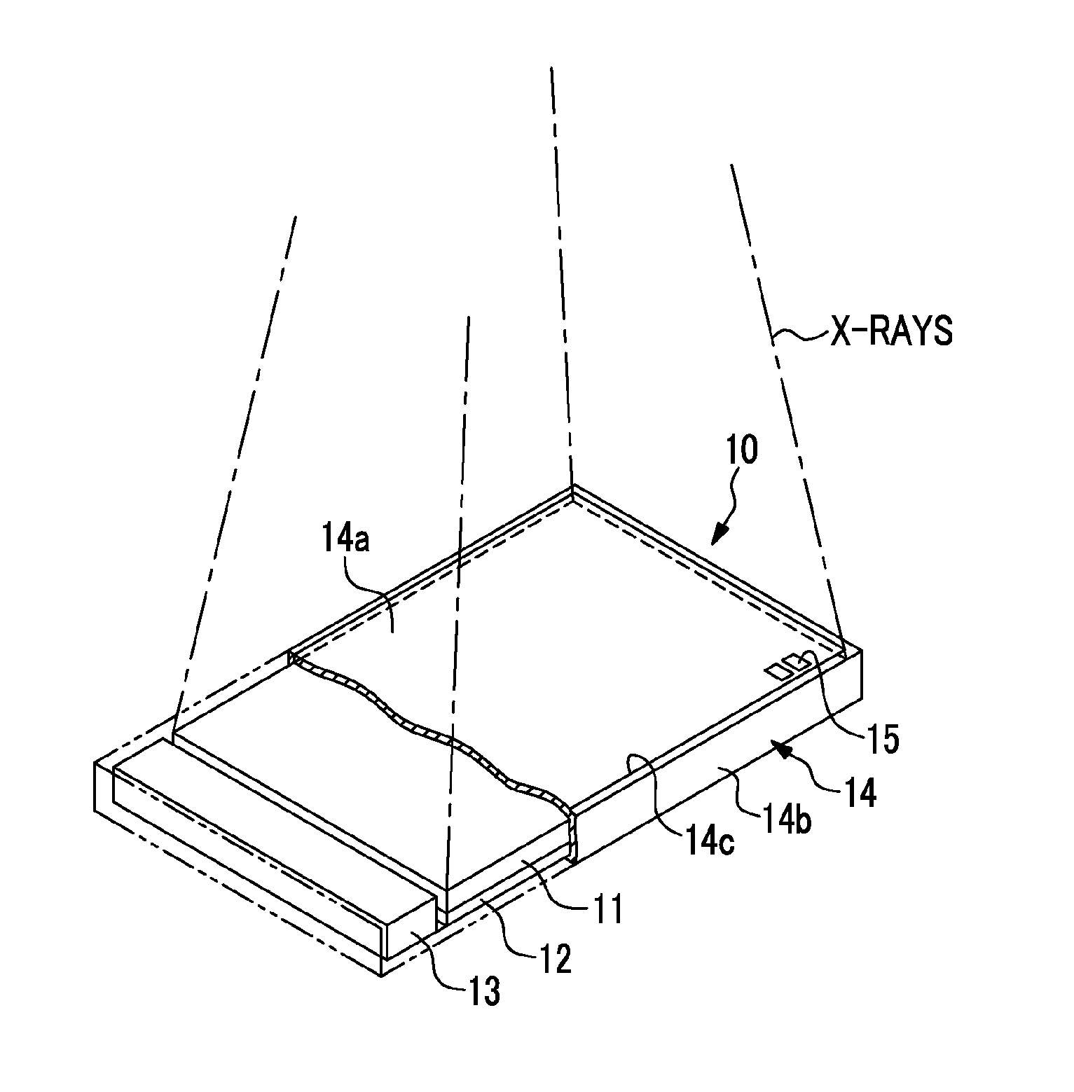
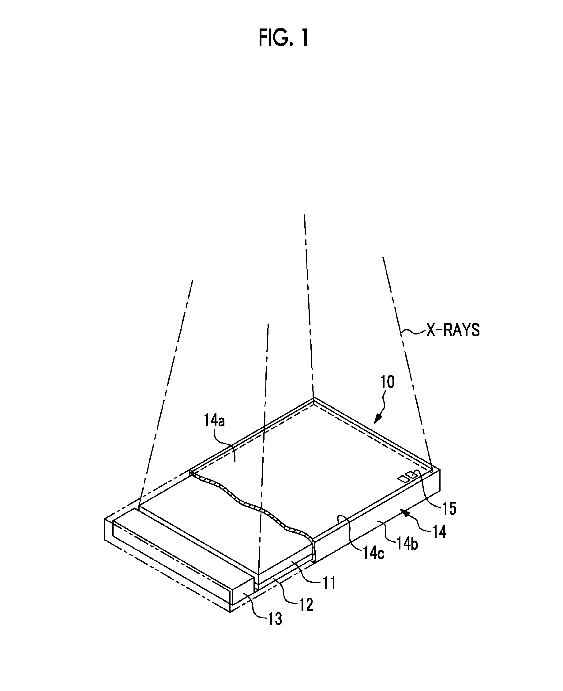
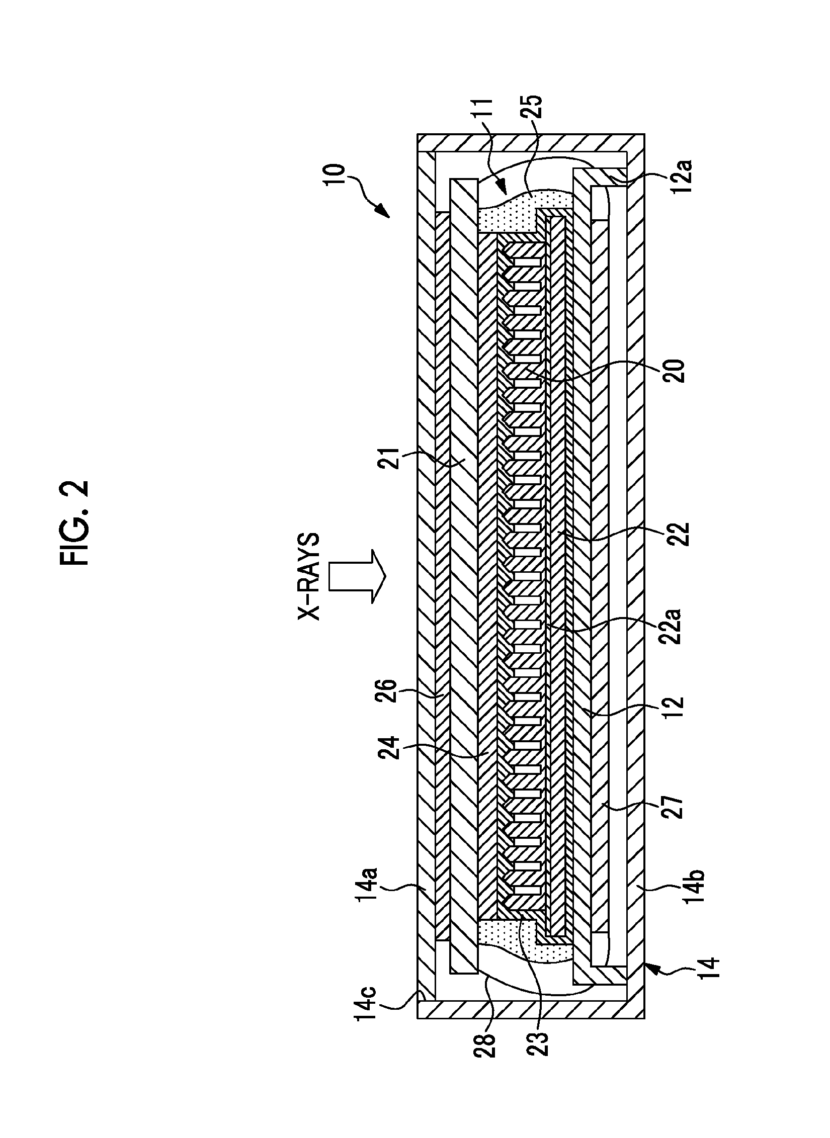
The present invention provides a radiological image detection apparatus that can improve sensitivity and reduce ghost. This is achieved by setting certain conditions, such as I2 / I1≧0.1 and 540 nm≦WP≦570 nm, based on the maximum emission intensity of the scintillator, wavelength at which the maximum emission intensity is obtained, and the emission intensity at the wavelength of 400 nm. This allows for better image quality and reduced blurring.

Problems solved by technology

However, although the sensitivity of a radiological image detection apparatus having a scintillator manufactured using a manufacturing method disclosed in JP2009-47577A is enhanced by the improvement in the light transmittance of the scintillator, the generation of a residual image called a ghost becomes a problem.
JP2009-47577A does not disclose a method of reducing the ghost while improving the sensitivity.

Method used


Image

  • Radiological image detection apparatus and method of manufacturing the same
  • Radiological image detection apparatus and method of manufacturing the same
  • Radiological image detection apparatus and method of manufacturing the same

Examples


examples

[0064]Hereinafter, the present invention will be specifically described through examples. However, the present invention is not limited to these examples.

first example

[0065]Hereinafter, a first example of the scintillator of the present invention will be described. A surface protective film having a thickness of about 10 μm was formed by performing vapor deposition of poly-para-xylene on a support substrate formed of aluminum. This support substrate was put into the chamber of a vapor deposition apparatus, and thallium-activated cesium iodide (scintillator) having a thickness of about 650 μm was deposited on the substrate protective film by performing co-deposition with a material in which cesium iodide and thallium iodide were mixed. In this case, the amount of thallium iodide was adjusted so that the Tl / Cs ratio became 0.01.

[0066]Then, the support substrate was taken out from the chamber and was put into the heat treatment furnace, and an annealing process was performed for 2 hours at a temperature of 200° C. in a nitrogen atmosphere. Then, the support substrate was taken out from the heat treatment furnace and vapor deposition of poly-para-xyl...

second example

[0068]As a second example, a scintillator was manufactured as in the first example. In this case, the temperature of the annealing process was 150° C. (processing time was 2 hours).


PUM


Abstract

A ghost is reduced while improving the sensitivity. A scintillator has a plurality of columnar crystals formed of thallium-activated cesium iodide, and converts X-rays into visible light and emits the visible light from the distal end of the columnar crystal. The photoelectric conversion panel has a plurality of photodiodes formed of amorphous silicon to generate electric charges by detecting the visible light emitted from the scintillator. Assuming that the maximum emission intensity of the scintillator is I1, a wavelength at which the maximum emission intensity is obtained is WP, and the emission intensity at a wavelength of 400 nm is I2, I2 / I1≧0.1 and 540 nm≦WP<570 nm are satisfied.

Description

BACKGROUND OF THE INVENTION[0001]1. Field of the Invention[0002]The present invention relates to a radiological image detection apparatus that detects a radiological image and a method of manufacturing the same.[0003]2. Description of the Related Art[0004]In recent years, in the medical field, a radiation detection apparatus that detects a radiation (for example, X-rays), which is emitted from a radiation source toward an imaging region of a patient and is transmitted through the imaging region, and converts the radiation into electric charges and generates image data indicating a radiological image of the imaging region based on the electric charges is used to perform diagnostic imaging. There are a direct conversion type radiation detection apparatus, which directly converts a radiation into electric charges, and an indirect conversion type radiation detection apparatus, which converts a radiation into visible light first and converts the visible light into electric charges.[0005]...

Claims


Application Information

Patent Timeline
IPC IPC(8): G01T1/20H01L31/0232
CPCG01T1/2006H01L31/02322H01L27/14663G01T1/202
Inventor ANZAI, AKIHIROKATO, MUNETAKA
Owner FUJIFILM CORP
Learn More