Plasma CVD apparatus, plasma CVD method, reactive sputtering apparatus, and reactive sputtering method

a technology of plasma cvd and apparatus, which is applied in the field of plasma cvd method, reactive sputtering apparatus, and plasma cvd method, can solve the problems of loss of consistency in film deposition speed and film quality, poor film quality, and reduced productivity, so as to reduce deficiency, suppress contamination of electrode surface, and high quality

Inactive Publication Date: 2014-01-23
TORAY IND INC
View PDF1 Cites 11 Cited by
  • Summary
  • Abstract
  • Description
  • Claims
  • Application Information

AI Technical Summary

Benefits of technology

[0031]The present invention provides a plasma CVD apparatus and a reactive sputtering apparatus for depositing a thin film on a surface of a long substrate while the long substrate is being conveyed, wherein abnormal discharge is reduced, contamination of the electrode surface is suppressed, and consistency of the film deposition speed and quality is secured. Use of the plasma CVD apparatus and the reactive sputtering apparatus of the present invention enables production of a high quality thin film with reduced deficiency since inconsistency in the film deposition speed and the film quality by the contamination of the electrode surface can be suppressed, and in particular, since the film can be deposited under the condition wherein film contamination with high molecular weight substances and particles unnecessary for the plasma CVD is suppressed.

Problems solved by technology

Entering of these particles in the thin film during the deposition results in the poor film quality and these particles also deform shape of the discharge electrode surface by depositing on the surface of the discharge electrode.
The deformation of the discharge electrode surface by the deposition of the particles on the surface results in the change of the electric field generated between the discharge electrode and the substrate, and hence, in the loss of the consistency in the film deposition speed and the film quality.
In addition, more frequent cleaning of the apparatus will be required for the removal of the particles, and this results in the reduced productivity.
The situation is similar in the reactive sputtering, and in the reactive sputtering of an insulator material, the insulator material is deposited also on the target surface with the progress in the sputtering, and this leads to change in the electric field on the target surface, causing problems such as the loss of film consistency and generation of arc discharge.
However, patent document 1 does not clearly describe such exhausting method.
Patent document 2, however, does not disclose any structural countermeasure for the particles.
Provision of such protrusion like a pipe near the plasma area may cause abnormal discharge especially in the use of radio frequency power.

Method used


Image

  • Plasma CVD apparatus, plasma CVD method, reactive sputtering apparatus, and reactive sputtering method
  • Plasma CVD apparatus, plasma CVD method, reactive sputtering apparatus, and reactive sputtering method
  • Plasma CVD apparatus, plasma CVD method, reactive sputtering apparatus, and reactive sputtering method

Examples


example 1

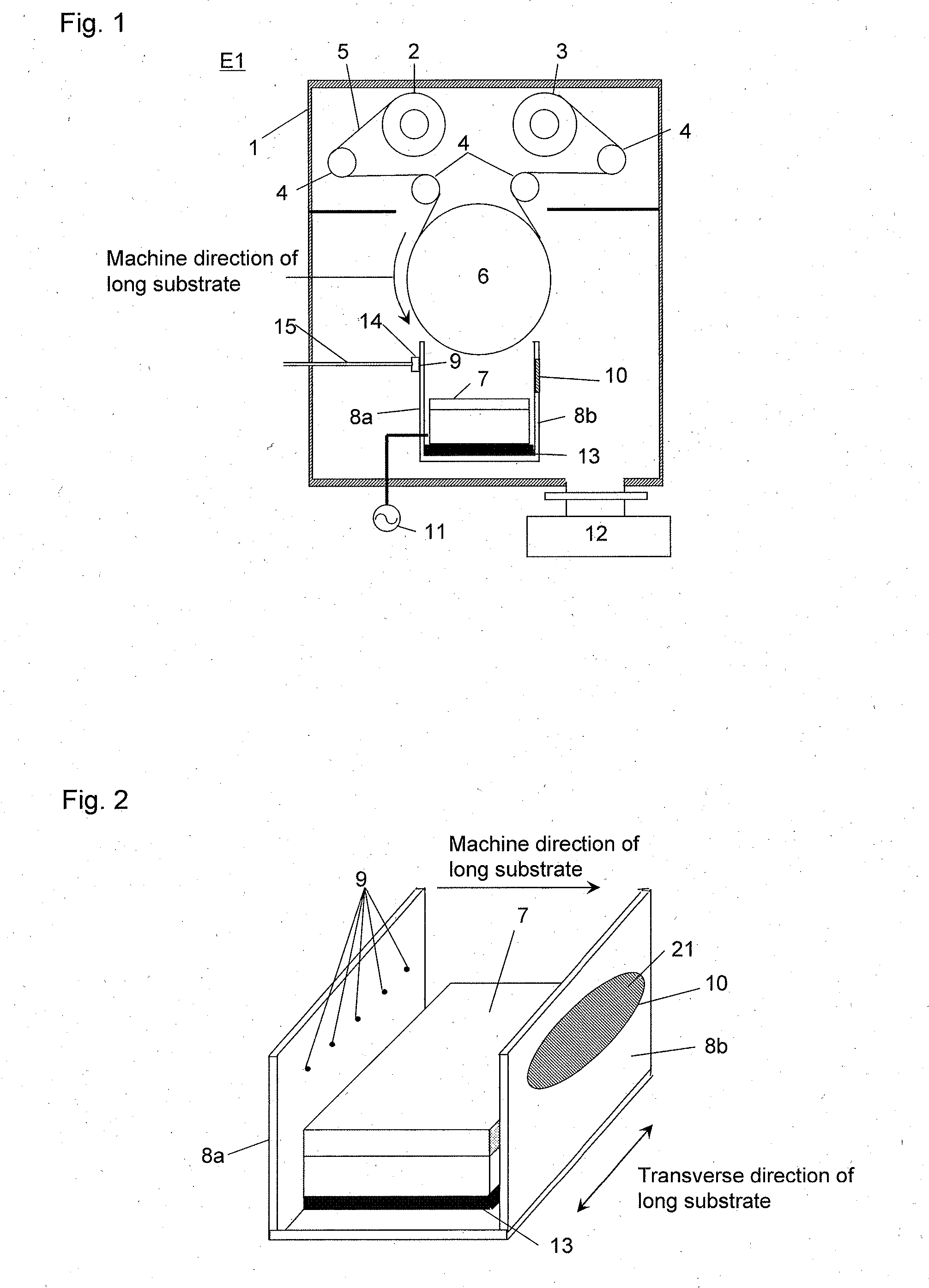
[0155]A silicon oxide film was formed by using the plasma CVD apparatus E1 shown in FIG. 1 in the method for forming the silicon oxide film according to the first embodiment. The plasma during the formation of the silicon oxide film and the electrode after the film deposition were examined.

[0156]In the plasma CVD apparatus E1, the main roll 6 had a diameter of 500 mm and a width of 340 mm. The plasma generation electrode 7 was formed by combining a titanium plate having a length of 236 mm, a width of 80 mm, and a thickness of 6 mm and a SUS box having a length of 236 mm, a width of 80 mm, and a height of 30 mm. Cooling water was circulated in the SUS box for the cooling of the titanium plate. The side walls 8a and 8b had a thickness of 3 mm. The height of the side walls 8a and 8b measured from the surface of the plasma generation electrode 7 on the main roll side was 50 mm, and the length in transverse direction was 248 mm. The side wall in the upstream side in the machine direction...

example 2

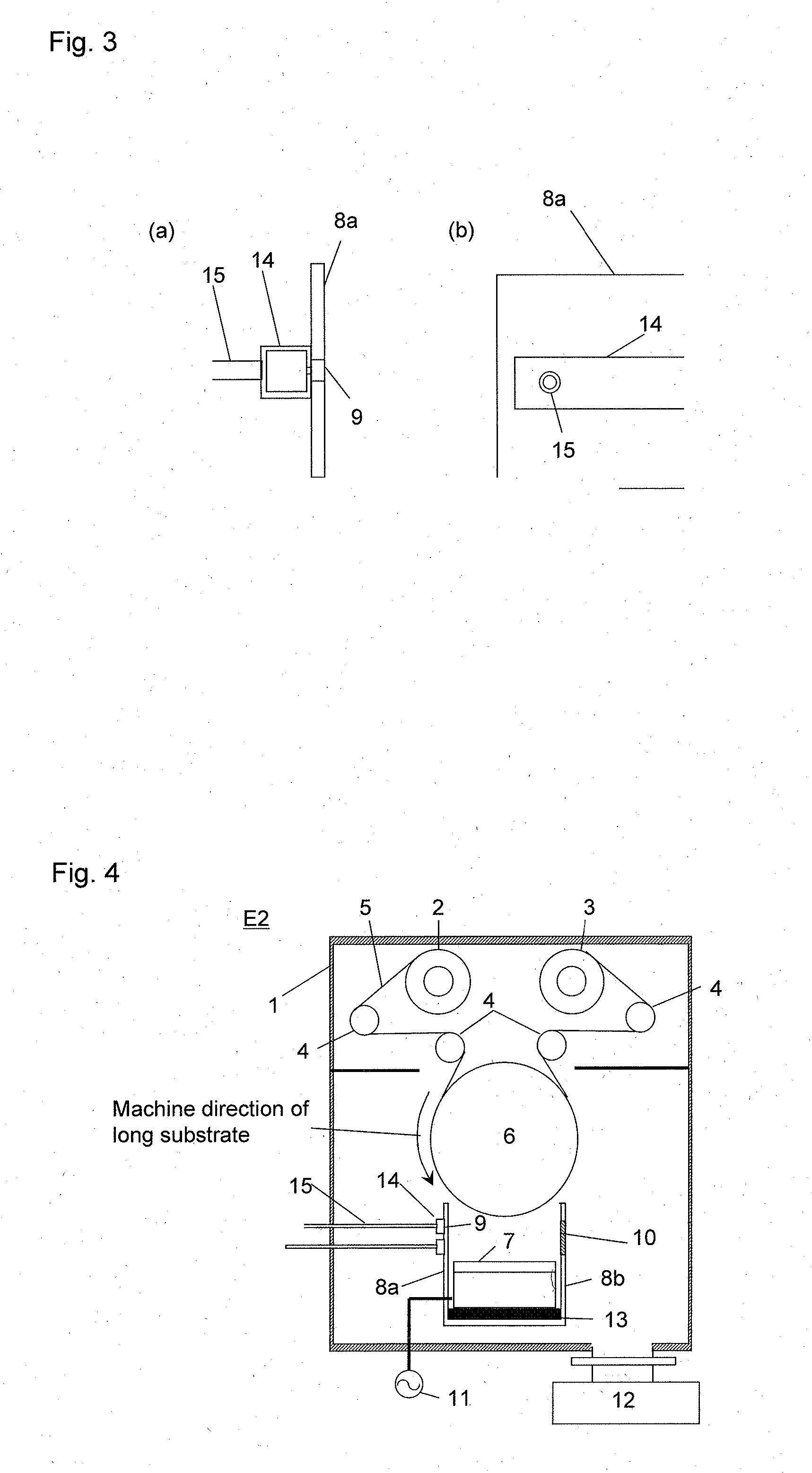
[0161]A silicon oxide film was formed by using the plasma CVD apparatus E2 shown in FIG. 4 in the method for forming the silicon oxide film according to the second embodiment. The plasma during the formation of the silicon oxide film and the electrode after the film deposition were examined. The row of the gas supply holes 9 for supplying the source gas was provided at the same position as the Example 1. Another row of gas supply holes 9 was formed at a position 9 mm from the row of the gas supply holes 9 for supplying the source gas on the side of the plasma discharge electrode 7, and Ar which was different from the carrier gas used was introduced from this row of the gas supply holes. 0.1 g / min of HMDSO was vaporized in a vaporizer (not shown) by using 50 sccm of Ar (carrier gas) and this gas mixture was further mixed with 100 sccm of oxygen for use as the source gas. 50 sccm of Ar in addition to the source gas was supplied from the lower row of the gas supply holes as described a...
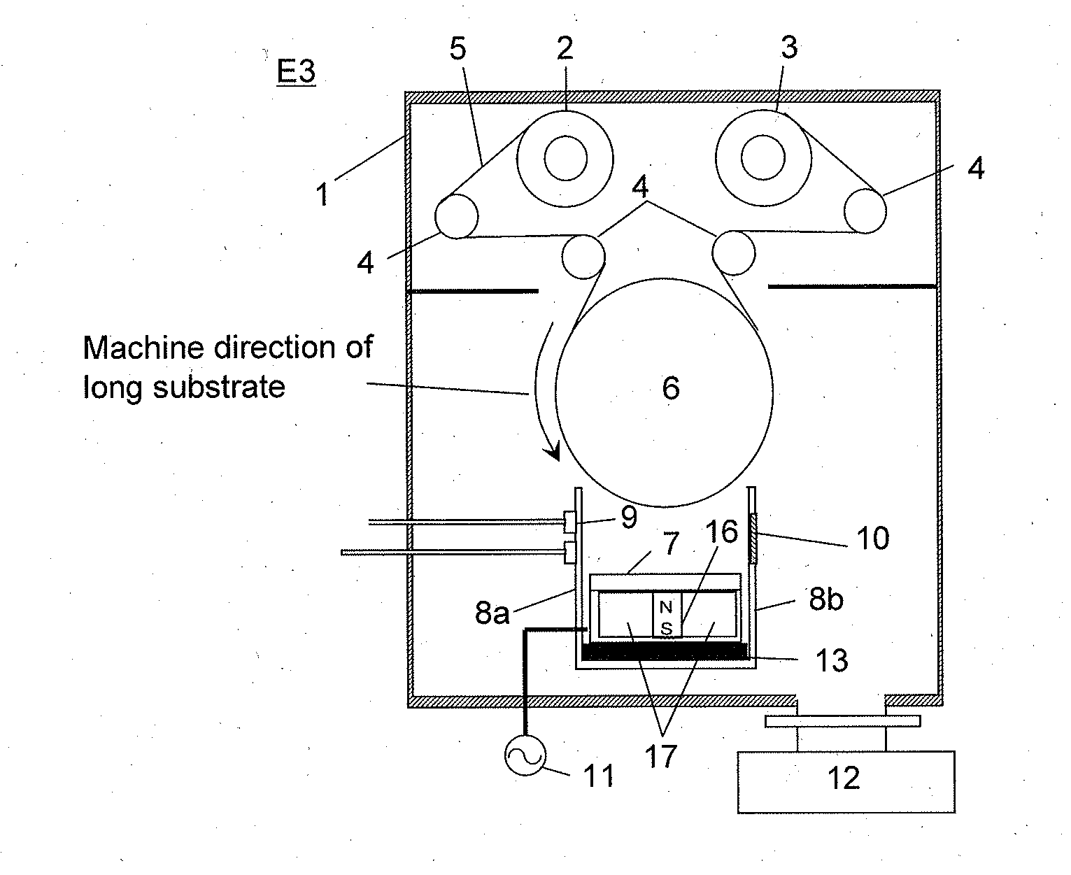
example 3

[0163]A silicon oxide film was formed by using the plasma CVD apparatus E3 shown in FIG. 5 in the method for forming the silicon oxide film according to the third embodiment, and the plasma during the deposition of the silicon oxide film and the electrode after the deposition of the silicon oxide film were observed. A neodymium magnet 16 having a width of 10 mm and a height of 15 mm was provided in the interior of the box of SUS in the plasma generation electrode 7, and cooling water was circulated in the cooling water pathway 17. The procedure of Example 2 was repeated for other aspects of this Example.

[0164]The film deposition speed was 45 nm×m / min without the magnet, and film deposition speed increased to 110 nm×m / min by the provision of the magnet. In addition, a stable film deposition with no abnormal discharge could be conducted as shown in Table 2. Contamination of the electrode after the film deposition was also reduced.


PUM

PropertyMeasurementUnit
pressureaaaaaaaaaa
inner diameteraaaaaaaaaa

Abstract

A plasma CVD apparatus comprising a vacuum chamber, and a main roll and a plasma generation electrode in the vacuum chamber, wherein a thin film is formed on a surface of a long substrate which is conveyed along the surface of the main roll is provided. At least one side wall extending in transverse direction of the long substrate is provided on each of the upstream and downstream sides in the machine direction of the long substrate, and the side walls surrounds the film deposition space between the main roll and the plasma generation electrode. The side walls are electrically insulated from the plasma generation electrode. The side wall on either the upstream or the downstream side in the machine direction of the long substrate is provided with at least one raw of gas supply holes formed by gas supply holes aligned in the transverse direction of the long substrate.

Description

CROSS REFERENCE TO RELATED APPLICATIONS[0001]This application is the U.S. National Phase application of PCT / JP2012 / 053403, filed Feb. 14, 2012, and claims priority to Japanese Patent Application No. 2011-077708, filed Mar. 31, 2011, Japanese Patent Application No. 2011-077709, filed Mar. 31, 2011, and Japanese Patent Application No. 2011-077710, filed Mar. 31, 2011, the disclosures of each of which are incorporated herein by reference in their entireties for all purposes.FIELD OF THE INVENTION[0002]This invention relates to a plasma CVD apparatus wherein plasma is generated in the gap between a long substrate and a plasma generation electrode, and chemical reaction of the source gas is promoted by using the thus generated plasma to thereby form a thin film on the surface of the long substrate. This invention also relates to a plasma CVD method, a reactive sputtering apparatus, and a reactive sputtering method.BACKGROUND OF THE INVENTION[0003]Various types of plasma CVD apparatus and...

Claims


Application Information

Patent Timeline
Patent Type & Authority Applications(United States)
IPC IPC(8): C23C14/00C23C16/455
CPCC23C14/0063C23C16/455C23C14/562C23C16/50C23C16/401C23C16/402C23C16/545H01J37/32559H01J37/32568H01J37/32752H01J37/3277H01J37/3405H01J37/3417H01J2237/3321H01J2237/3325C23C14/0068C23C16/45517C23C14/34
Inventor EJIRI, HIROESAKAMOTO, KEITARONOMURA, FUMIYASUUEDA, MASANORI
Owner TORAY IND INC
Why Eureka
Try Eureka