Method for making a two-layer capacitive touch sensor panel

a capacitive touch sensor and capacitive technology, applied in the field of two-layer capacitive touch sensor panels and to the panel, can solve the problems of high cost, undesirable thickness and heavy weight of the cover/sensor module, and reduce the thickness and weight of the sensor panel

Inactive Publication Date: 2014-02-13
M SOLV
View PDF8 Cites 36 Cited by
  • Summary
  • Abstract
  • Description
  • Claims
  • Application Information

AI Technical Summary

Benefits of technology

[0041]A further advantage of the invention is that it enables a very thin dielectric layer to be used, eg having a thickness of only 10s of μms. In a preferred arrangement, the dielectric layer may have a thickness off 10 μm or less. This further reduces the thickness and weight of the sensor panel.
[0042]Other preferred and optional features of the invention will be apparent from the following description and from the subsidiary claims of the specification.

Problems solved by technology

Such a “dual component” arrangement can lead to a cover / sensor module that is undesirably thick and heavy.
Both of these manufacturing technologies lead to a cover / sensor module that is relatively thick and heavy because it consists of two components.
Such multi-step processes which have to be repeated for every material layer requiring patterning have a high cost associated with them as large quantities of capital equipment are needed and large amounts of chemicals are required.
A major factor contributing to the high cost of ownership is that for each sensor design special costly masks are required for every layer to be patterned.

Method used


Image

  • Method for making a two-layer capacitive touch sensor panel
  • Method for making a two-layer capacitive touch sensor panel
  • Method for making a two-layer capacitive touch sensor panel

Examples


Embodiment Construction

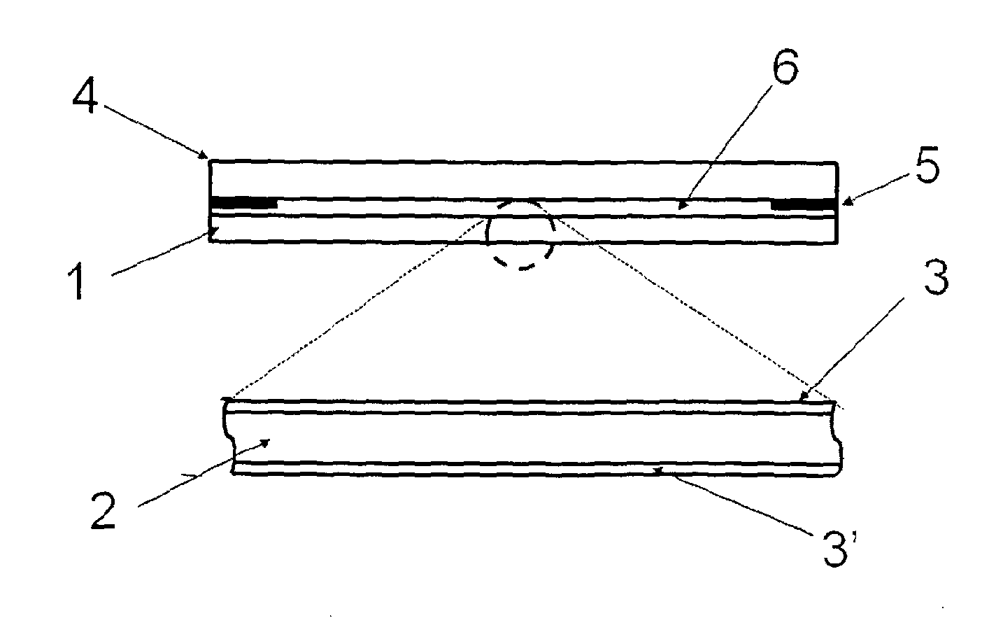
[0056]FIG. 1: This shows the construction of a first known type of cover / sensor module as used in many hand held devices with capacitive touch capability. Capacitive sensor 1 is of a two-layer type and consists of a transparent dielectric material 2 such as plastic or glass with a transparent conducting layer (TCL) on each side 3, 3′. Electrode patterns are formed in the TCLs to create the capacitive sensor. Cover sheet 4 is made of either glass or plastic and may have decorative ink 5 applied around the border. The capacitive sensor 1 is generally bonded to the cover sheet glass by means of UV curing glue 6 that fills the gap between the cover sheet 4 and the sensor,

[0057]FIG. 2: This shows the detail of the construction of the type of sensor 1 shown in FIG. 1. The dielectric substrate 2 for the capacitive sensor is generally made of glass or plastic. In the case of a glass substrate the thickness is generally in the range 0.33 to 0.7 mm. In the case of a plastic substrate the thic...


PUM


Abstract

A method of fabricating a two-layer capacitive touch sensor panel comprising the following steps: a) depositing a first transparent electrically conductive layer on a transparent cover sheet; b) forming a pattern in the transparent electrically conductive layer to create a first set of discrete electrode structures; c) depositing a transparent dielectric layer over the discrete electrode structures; d) depositing a second transparent electrically conductive layer onto the transparent dielectric layer; e) forming a pattern in the transparent electrically conductive layer to create further discrete electrode structures by laser ablation, this pattern either not penetrating or penetrating only part way through the dielectric layer so as to avoid damaging the first set of discrete electrode structures; f) forming electrical connections or vias between the two transparent electrically conductive layers through the dielectric layer; and g) forming electrical connections between the transparent electrically conductive layer(s) and an electrical track or busbar formed at the periphery of the panel.) The method provides a maskless, chemical free way to fabricate a two-layer “cover integrated” sensor. A two-layer capacitive touch sensor panel fabricated by this method is also described

Description

TECHNICAL FIELD[0001]This invention relates to a method of making a two-layer capacitive touch sensor panel and to a panel made by the method.BACKGROUND ARTBackground[0002]There is a great desire to incorporate capacitive touch sensors with multi touch capability into hand held devices such as mobile smart phones, MP3 players, PDAs, tablet PCs, etc. Such devices generally have a transparent front cover sheet that is made of glass or plastic onto the rear of which a two-layer transparent capacitive sensor is bonded. Such a “dual component” arrangement can lead to a cover / sensor module that is undesirably thick and heavy. To reduce the thickness and weight it is desirable to form the sensor directly on the cover sheet. This “cover integrated” sensor arrangement leads to a module that is substantially thinner than can be made by other means[0003]Prior art in the “dual component” area generally involves making a two-layer capacitive sensor and cover sheet as separate items and then lami...

Claims


Application Information

Patent Timeline
Patent Type & Authority Applications(United States)
IPC IPC(8): H05K3/46H05K1/02
CPCH05K1/0298H05K3/4644G06F2203/04103G06F3/0445G06F3/044
Inventor PEDDER, JAMES
Owner M SOLV
Why Eureka
Try Eureka