Method for fabricating one-dimensional metallic nanostructures

a technology of metallic nanostructures and nanowires, applied in the direction of superimposed coating processes, coatings, semiconductor devices, etc., can solve the problems of limited nanowire width, complicated process, and expensive equipment for the method, and achieve the effect of reducing fabrication costs and expanding industrial applications

Inactive Publication Date: 2014-02-20
NAT CHIAO TUNG UNIV
View PDF6 Cites 9 Cited by
  • Summary
  • Abstract
  • Description
  • Claims
  • Application Information

AI Technical Summary

Benefits of technology

[0009]The primary objective of the present invention is to provide a method for fabricating one-dimensional metallic nanostructures, which uses a simple DC or AC electroplating system to form flexib...

Problems solved by technology

However, the method needs expensive equipment and uses a complicated process.
Besides, the width of the nanowire is limited by the wavelength of the laser light.
The metallic nanostructure fabricated by the method is likely to have many tumbling defects.
B...

Method used


Image

  • Method for fabricating one-dimensional metallic nanostructures
  • Method for fabricating one-dimensional metallic nanostructures
  • Method for fabricating one-dimensional metallic nanostructures

Examples


Embodiment Construction

[0019]Nanomaterials have superior performance and have been applied to various fields. Among nanomaterials, one-dimensional metallic nanostructures challenge researchers most severely and have the largest space to develop. The current technologies for fabricating one-dimensional metallic nanostructures suffer from high fabrication cost, harsh technical difficulties, and rare technical breakthroughs. Therefore, the present invention proposes a novel method for fabricating one-dimensional metallic nanostructures to overcome the problems of the conventional technologies.

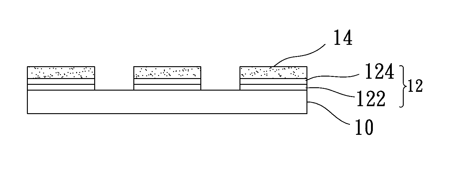
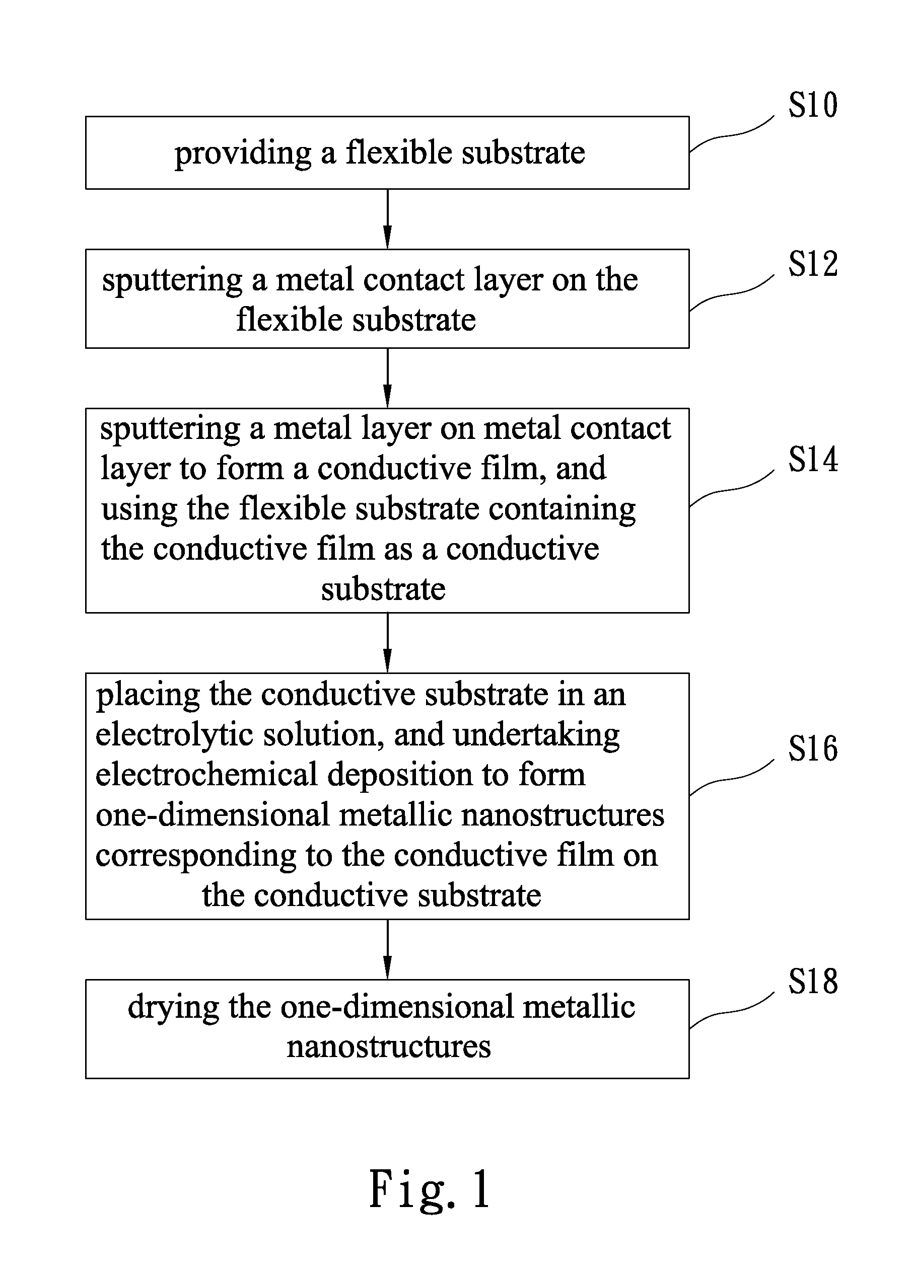
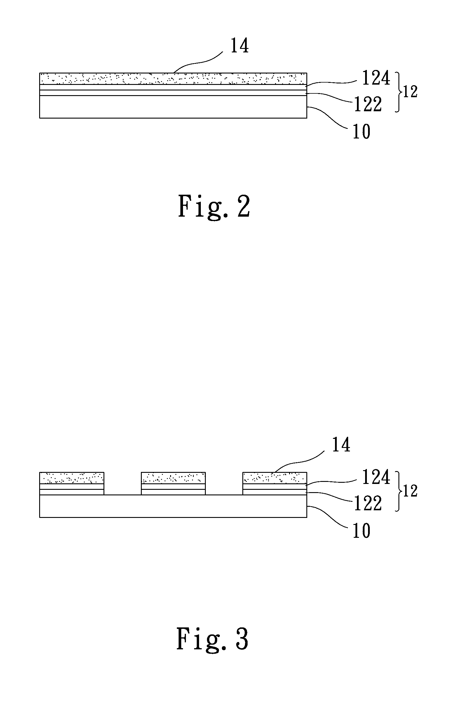
[0020]Refer to FIG. 1 showing a flowchart of a method for fabricating one-dimensional metallic nanostructures according to one embodiment of the present invention. Also refer to FIG. 2 a diagram schematically showing one-dimensional metallic nanostructures fabricated according to one embodiment of the present invention. In Step S10, provide a flexible substrate 10, such as a plastic substrate (e.g. a PET substrate), a c...


PUM

PropertyMeasurementUnit
Temperatureaaaaaaaaaa
Lengthaaaaaaaaaa

Abstract

A method for fabricating one-dimensional metallic nanostructures comprises steps: sputtering a conductive film on a flexible substrate to form a conductive substrate; placing the conductive substrate in an electrolytic solution, and undertaking electrochemical deposition to form one-dimensional metallic nanostructures corresponding to the conductive film on the conductive substrate. The method fabricates high-surface-area one-dimensional metallic nanostructures on a flexible substrate, exempted from the high price of the photolithographic method, the complicated process of the hard template method, the varied characteristic and non-uniform coating of the seed-mediated growth method.

Description

BACKGROUND OF THE INVENTION[0001]1. Field of the Invention[0002]The present invention relates to a one-dimensional metallic nanostructure, particularly to a method using an electroplating process to form one-dimensional metallic nanostructures on a flexible substrate.[0003]2. Description of the Related Art[0004]To miniaturize various products, the electronics has progressed from the micron age to the nano age. There have been various nanomaterials, including metallic nanomaterials, semiconductor nanomaterials, ceramic nanomaterials, and polymeric nanomaterials. According to their geometrical attributes, nanomaterials may be categorized into zero-dimensional nanomaterials, one-dimensional nanomaterials, two-dimensional nanomaterials, etc. The up-to-date methods for growing a nanostructure on a substrate include the photolithographic method, the hard template method, the seed-mediated growth method and the de-alloy method.[0005]In the photolithographic method, a photoresist material i...

Claims


Application Information

Patent Timeline
IPC IPC(8): C23C28/02C25D7/12C25D5/56C25D5/54B82Y40/00B82Y99/00
CPCB82Y40/00C25D3/48C25D5/02C25D5/34C25D7/0607C23C28/023C25D7/123
Inventor CHEN, YU-LIANGCHIEN, NAI-YINGCHIU, HSIN-TIENLEE, CHI-YOUNG
Owner NAT CHIAO TUNG UNIV
Why Eureka
Try Eureka