

Microcontroller
a microcontroller and microcontroller technology, applied in the field of microcontrollers, can solve the problems of limited and achieve the effect of increasing flexibility in timing of power supply stoppage and reducing power consumption of microcontrollers
- Summary
- Abstract
- Description
- Claims
- Application Information
AI Technical Summary
Benefits of technology
Problems solved by technology
Method used
Image


Examples
embodiment 1
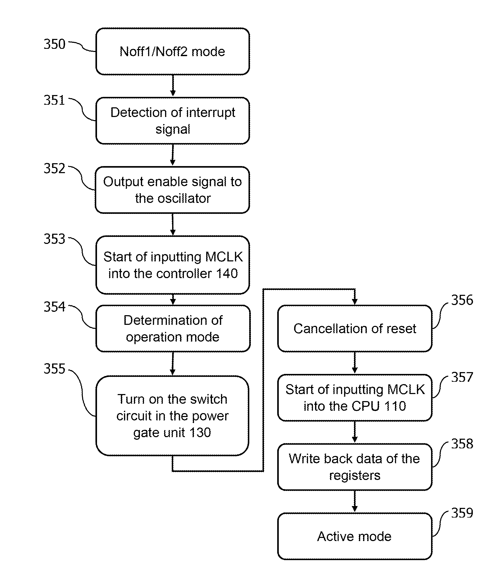
[0046]A configuration and operation of a microcontroller will be described with reference to FIG. 1. FIG. 1 is a block diagram of a microcontroller 100.
[0047]The microcontroller 100 includes a central processing unit (CPU) 110, a bus bridge 111, a random access memory (RAM) 112, a memory interface 113, a controller 120, an interrupt controller 121, an input / output interface (I / O interface) 122, and a power gate unit 130.
[0048]The microcontroller 100 further includes a crystal oscillation circuit 141, a timer circuit 145, an I / O interface 146, an I / O port 150, a comparator 151, an I / O interface 152, a bus line 161, a bus line 162, a bus line 163, and a data bus line 164. Further, the microcontroller 100 includes at least connection terminals 170 to 176 as connection parts with external devices. Note that the connection terminals 170 to 176 each represent one terminal or a terminal group including plural terminals.
[0049]FIG. 2 is a layout example of circuit blocks included in the micr...
embodiment 2
[0106]A register including both a nonvolatile memory and a volatile memory will be described with reference to FIG. 6.
[0107]FIG. 6 is a circuit diagram of a register including both a nonvolatile memory and a volatile memory. FIG. 6 illustrates a register 200 having a one-bit memory capacity. The register 200 includes memory circuits 201 and 202. The memory circuit 201 is a one-bit volatile memory, while the memory circuit 202 is a one-bit nonvolatile memory. Note that the register 200 can include another component such as a diode, a resistor, or an inductor.
[0108]To the memory circuit 201 is given a low power supply potential VSS (hereinafter, referred to as VSS) and a high power supply potential VDD (hereinafter, referred to as VDD) as power supply potentials. The memory circuit 201 can store data during a period in which a potential difference between VDD and VSS is supplied as a power supply potential.
[0109]The memory circuit 202 includes a transistor 203, a transistor 204, a cap...
embodiment 3
[0128]A memory cell structure of the RAM 112 will be described with reference to FIG. 7. FIG. 7 is a circuit diagram of a memory cell 400 in the RAM 112. The memory cell 400 includes three transistors 401 to 403 and a capacitor 404. The memory cell 400 is connected to a bit line BL, a word line RWL, and a word line WWL. The word line RWL is a read word line, and the word line WWL is a write word line. In addition, VSS is supplied from a power supply line 405 to the memory cell 400. When VSS is a potential higher than 0 V, the potential of the power supply line 405 can be 0 V.
[0129]The bit line BL is connected to a read-out circuit and a write circuit of the RAM 112. In addition, the word lines RWL and WWL are connected to a row driver.
[0130]In order that the memory cell 400 can act as a nonvolatile memory circuit, the transistor 401 is preferably a transistor with extremely low off-state current, like the transistor 203 in the register 200. This is because the charge of the node FN ...
PUM
 Abstract
Description
Claims
Application Information