GROUP-IV SOLAR CELL STRUCTURE USING GROUP-IV or III-V HETEROSTRUCTURES

a solar cell and heterostructure technology, applied in the field of photovoltaic cells, can solve the problems of increasing relative power loss, limiting the number of subcells (also referred to as collecting junctions or subcell junctions), and reducing the efficiency of solar cells, so as to reduce the effective band gap, reduce the energy band gap, and increase the density of photogenerated and/or collected curren

Active Publication Date: 2014-03-20
THE BOEING CO
View PDF11 Cites 26 Cited by
  • Summary
  • Abstract
  • Description
  • Claims
  • Application Information

AI Technical Summary

Benefits of technology

[0029]According to the disclosure, energy wells comprising one or more group-IV semiconductor regions, with one of more compositions chosen to have a lower energy bandgap than adjacent regions, may be positioned in the main photogeneration layer or other group-IV photogeneration layer of a group-IV solar cell, such as the group-IV emitter or base of the solar cell, to lower the effective bandgap of the group-IV photogeneration layer, increasing the photogenerated and / or collected current density of the solar cell.
[0030]According to the disclosure, energy wells or low-bandgap absorber regions (LBARs) may be used in other subcells of the multijunction cell in which the group-IV solar cell is positioned, in order to modify the effective bandgap, light transmission, and photogenerated and collected current density in the other subcells, to achieve a trade-off between light transmitted by the other subcells to the group-IV subcell or subcells, light transmitted by the group-IV subcell of subcells to the other subcells, and the voltage, photogenerated current density, and collected current density of the group-IV subcell or subcells and the other subcells in the multijunction cell, to result in higher performance of the overall multijunction cell.
[0032]According to the disclosure, the group-IV solar cell may be combined with a passivation layer on the front or the back of the cell, to reduce surface minority-carrier recombination in the cell, chosen from a group including: a deposited amorphous silicon layer; a deposited amorphous germanium layer; a deposited amorphous layer containing carbon, silicon, and / or germanium; a dielectric layer such as silicon dioxide, silicon oxide, or silicon nitride; a deposited semiconductor layer such as zinc oxide or indium tin oxide; a chemical surface treatment such as hydrogen, fluorine, sulfur, or selenium deposited on the surface; and combinations of the above, in order increase photogenerated and collected current density, e.g., by increasing the current that can be collected from thick group-IV solar cell layers from carrier photogeneration by indirect energy transitions in the energy band structure of the group-IV solar cell.

Problems solved by technology

With multijunction cells, efficiency is limited by the requirement of low resistance interfaces between the individual cells to enable the generated current to flow from one cell to the next.
Another limitation to the multiple cell PV device, or multijunction cell, is that current output in each subcell must be the same for optimum efficiency in the series-connected configuration.
In addition, there has been a practical limit on the number of subcells (also referred to as collecting junctions or subcell junctions) employed, since the benefit of each successive subcell becomes smaller as the number of subcells increases, and each subcell has certain parasitic losses associated with it in practice, tending to counteract the greater efficiency that comes from dividing the incident spectrum into smaller energy ranges with a greater number of subcells.
The structures described above have relatively high current densities, which can present problems for current matching subcells that are poor current producers.
The comparatively high current densities and low voltages of these cells with 1 to 3 subcells result in greater relative power loss due to series resistance.
Further, subcell base thicknesses can be comparatively large, and some subcells have little excess photogenerated current density, both of which impair radiation resistance.
Limited excess photogenerated current density in low bandgap subcells can also impair the fill factor of the overall multijunction solar cell that they are in.

Method used


Image

  • GROUP-IV SOLAR CELL STRUCTURE USING GROUP-IV or III-V HETEROSTRUCTURES
  • GROUP-IV SOLAR CELL STRUCTURE USING GROUP-IV or III-V HETEROSTRUCTURES
  • GROUP-IV SOLAR CELL STRUCTURE USING GROUP-IV or III-V HETEROSTRUCTURES

Examples


Embodiment Construction

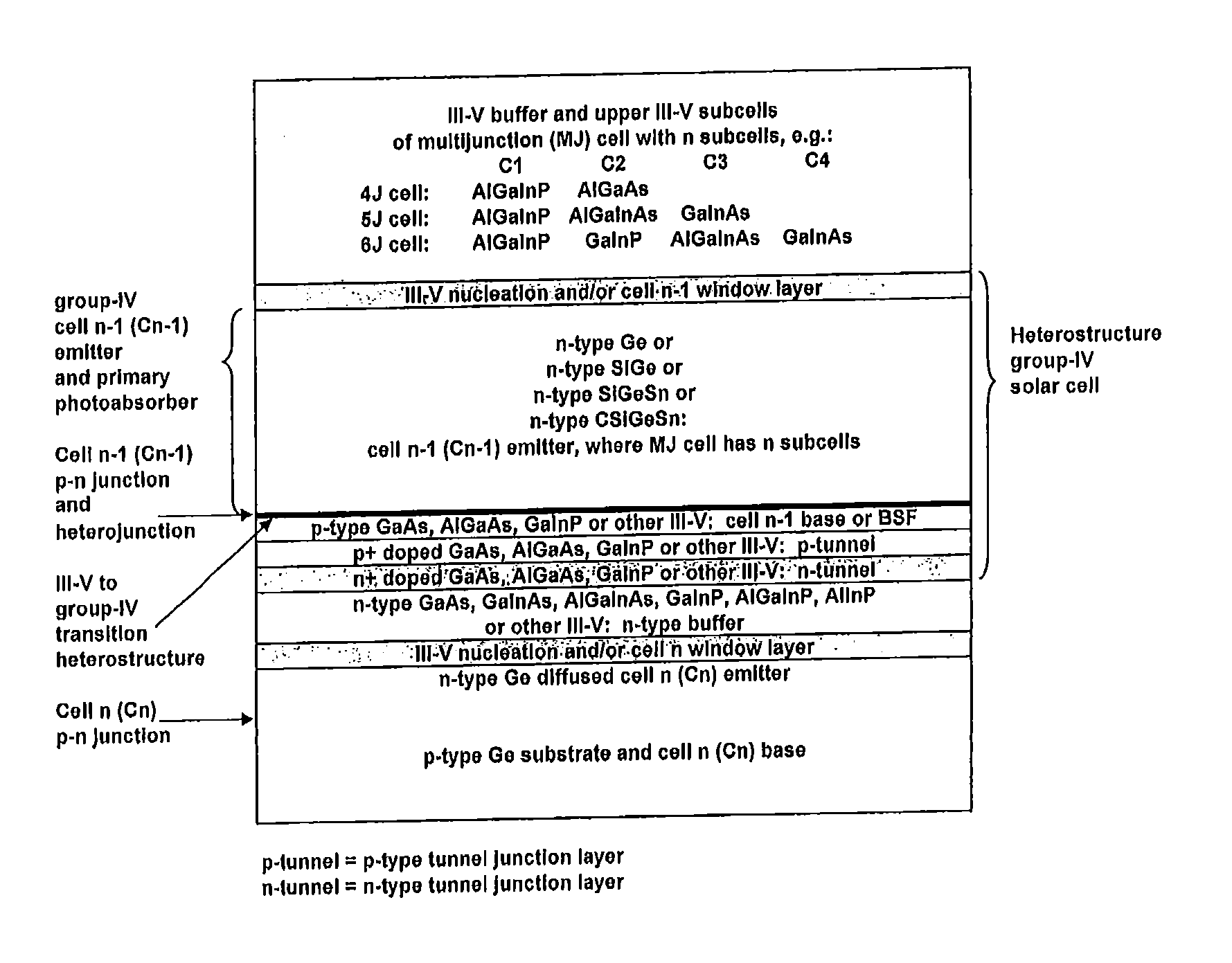
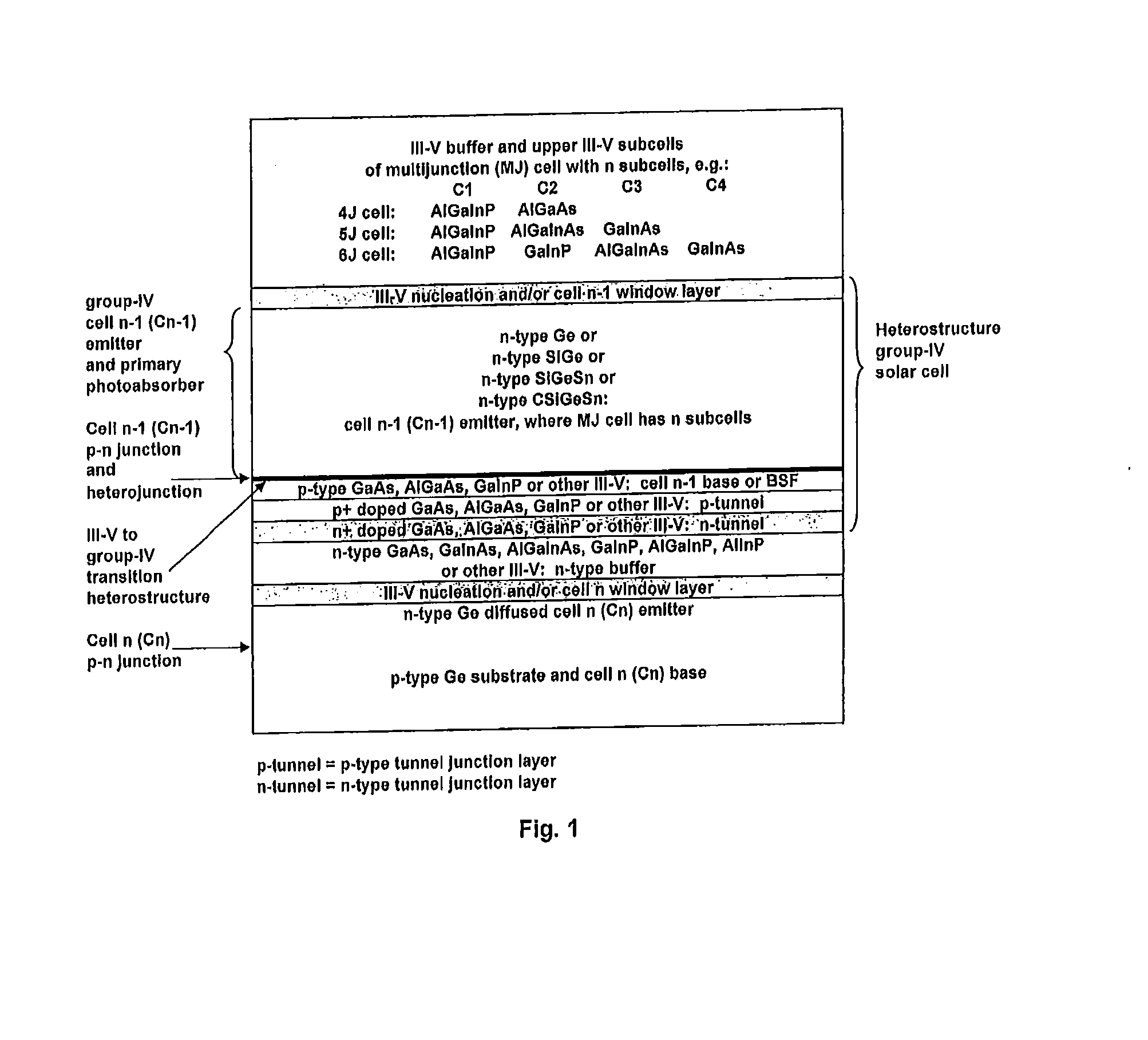
[0122]According to the present disclosure, systems and methods are disclosed for making significant improvements for terrestrial and non-terrestrial photovoltaic cells, such as, for example, concentrator solar cells and space solar cells, providing significantly higher efficiency than are available in today's most advanced solar cells. The approaches described herein make use of the lower-cost, more reliable, and more scalable processes of upright solar cell growth, and lattice-matched growth or metamorphic growth with small lattice mismatch, as opposed to the inverted cell growth and cell processing, and metamorphic growth with high lattice mismatch of inverted metamorphic cells.

[0123]The present disclosure allows the formation of multijunction cells, such as, for example, 3-junction (3J), 4-junction (4J), 5-junction (5J), 6-junction (6J), 7-junction (7J) solar cells, or cells with 8 junctions or more that incorporate a group-IV solar cell. Preferred cells comprise, for example, ep...


PUM


Abstract

Device structures, apparatuses, and methods are disclosed for photovoltaic cells that may be a single junction or multijunction solar cells, with at least one layer comprising a group-IV semiconductor in which part of the cell comprises a second layer comprising a III-V semiconductor or group-IV semiconductor having a different composition than the group-IV semiconductor of the first layer, such that a heterostructure is formed between the first and second layers.

Description

TECHNOLOGICAL FIELD[0001]The present disclosure relates to photovoltaic cells and their methods of manufacture and, more particularly, to improved single-junction cells or subcells in a multijunction photovoltaic (PV) cell, especially a solar cell, having multiple layers to form a heterostructure.BACKGROUND[0002]Advances in photovoltaic cells remain important for terrestrial and non-terrestrial applications. In the non-terrestrial environment of outer space, as well as terrestrial applications, photovoltaic cells offer a valuable means for providing power generation by converting the abundant resource of the sun's energy to electrical power.[0003]Irrespective of the application, and as with any energy generation system, efforts continue to increase the output and / or efficiency of PV cells. With respect to output, multiple cells or layers having differing energy bandgaps have been stacked so that each cell or layer can absorb a different part of the wide energy distribution of photon...

Claims


Application Information

Patent Timeline
Patent Type & Authority Applications(United States)
IPC IPC(8): H01L31/0264H01L31/06H01L31/0232H01L31/02
CPCH01L31/0725H01L31/074H01L31/078Y02E10/544H01L31/0687H01L31/0745H01L31/0443Y02P70/50
Inventor KING, RICHARD R.FETZER, CHRISTOPHER M.KARAM, NASSER H.
Owner THE BOEING CO
Why Eureka
Try Eureka