Transparent conductive laminate and transparent touch panel

a technology of transparent touch panel and conductive laminate, which is applied in the direction of conductive layers on insulating supports, paper/cardboard containers, instruments, etc., can solve the problems of disadvantageous breakage, low surface hardness and easy scratching of transparent organic polymer substrates

Inactive Publication Date: 2014-03-27
TEIJIN LTD
View PDF5 Cites 9 Cited by
  • Summary
  • Abstract
  • Description
  • Claims
  • Application Information

AI Technical Summary

Benefits of technology

[0041]According to the present invention, a transparent electroconductive laminate which does not cause cracking due to bending is provided. Furthermore, according to the present invention, a transparent touch panel, particularly a transparent touch panel of a resistive film system or a capacitance system, having such a transparent electroconductive laminate is provided.
[0042]More specifically, in the transparent electroconductive laminate of the present invention, a cured resin layer having specific properties and a transparent electroconductive layer are stacked on at least one surface of a transparent organic polymer substrate.

Problems solved by technology

Such a transparent organic polymer substrate is low in the surface hardness and susceptible to scratching, and therefore the surface of the transparent organic polymer substrate is coated with a resin layer called a cured resin layer.
However, the laminate obtained by coating a transparent organic polymer substrate with a hard cured resin layer becomes more brittle than a transparent organic polymer substrate itself not coated with a hard cured resin layer, and therefore is disadvantageously broken when bent.
This tendency is prominent in using a substrate having low mechanical strength, such as transparent organic polymer substrate formed of a low-molecular-weight polycarbonate resin or an amorphous polyolefin, and this problem has been considered to be difficult to solve.
Breakage of the laminate gives rise to reduction in the handleability at the production of a transparent panel, and is a fatal feature particularly to a substrate for a resistive film-type touch panel requiring mechanical strength.

Method used


Image

  • Transparent conductive laminate and transparent touch panel
  • Transparent conductive laminate and transparent touch panel

Examples


example 1

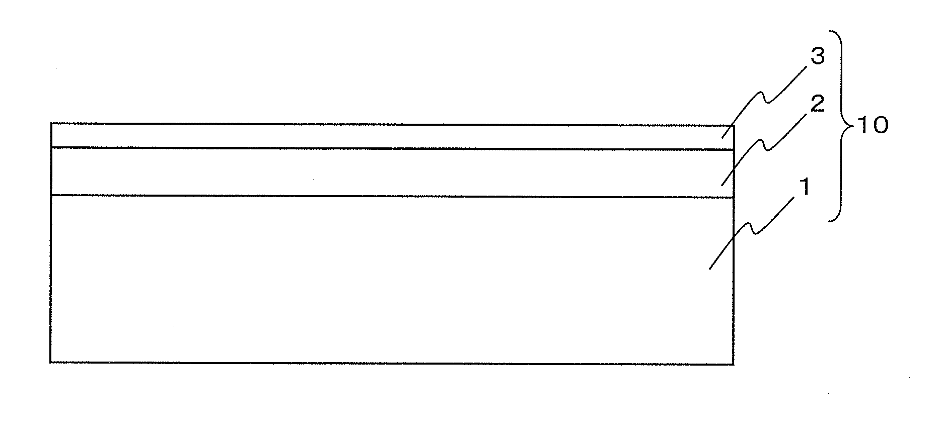
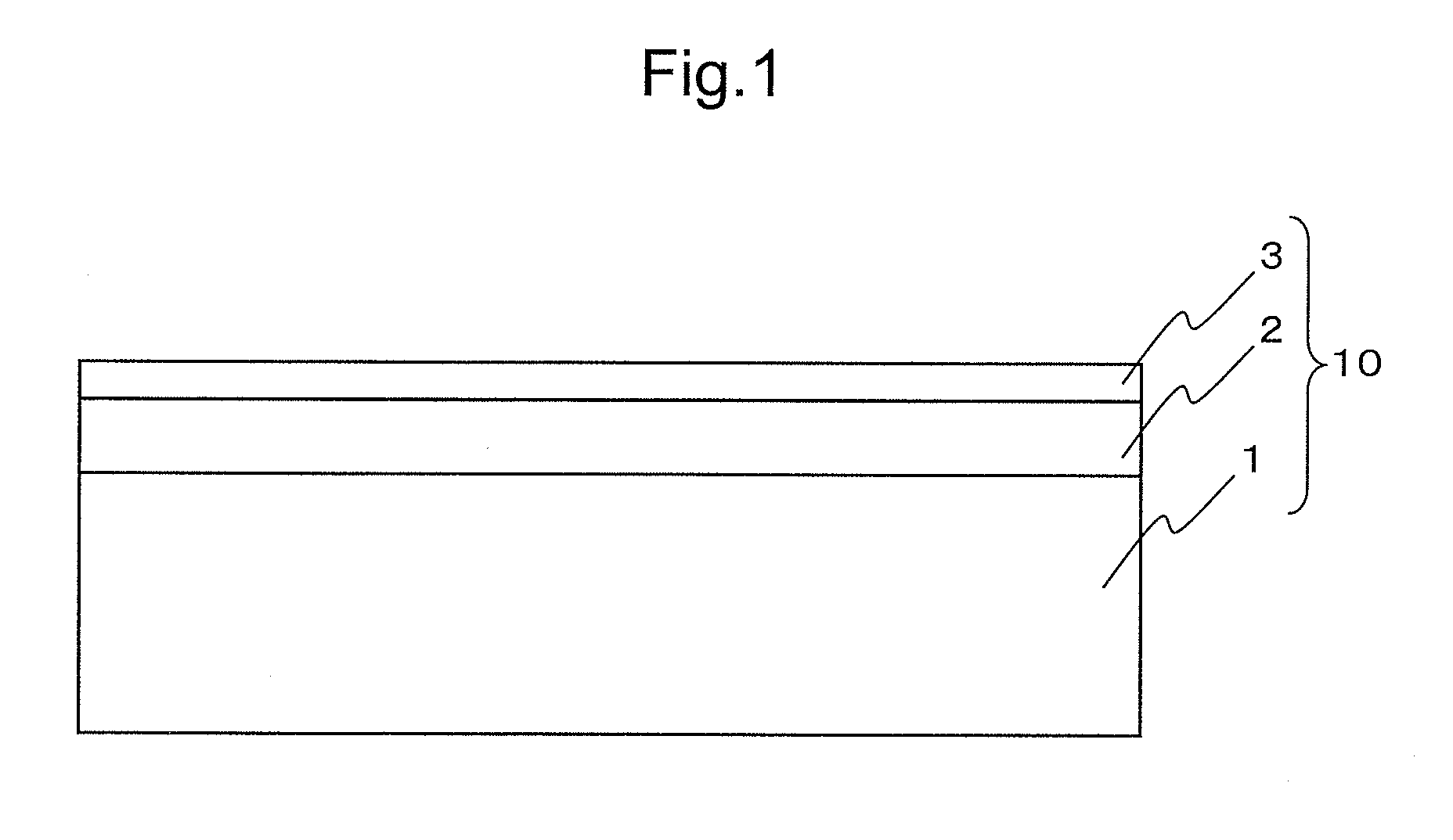
[0183]On one surface of a 100 μm-thick polycarbonate (PC) film prepared by a melting method (“PANLIGHT Film” D100, produced by Teijin Chemicals, Ltd., weight average molecular weight: 18,500, tensile elongation at break: 5%), Coating Solution P1 was coated by a bar coating method, irradiated with an ultraviolet ray and thereby cured to form a cured resin layer having a thickness of 3 μm. Separately from this, for an indentation hardness test, a sample of a cured resin layer having a thickness of 5 μm was prepared by the same method.

[0184]Furthermore, an ITO layer was formed on the cured resin layer by a sputtering method using an indium oxide-tin oxide target having a composition of indium oxide and tin oxide in a weight ratio of 95:5 and having a filling density of 98% to produce a transparent electroconductive laminate used as a movable electrode substrate. The film thickness of the ITO layer formed was about 20 nm, and the surface resistance value after film formation was about 3...

example 2

[0187]A cured resin layer was formed in the same manner as Example 1 except for changing the thickness of the cured resin layer to 8 μm.

[0188]Furthermore, an ITO layer was formed in the same manner as Example 1. The film thickness of the ITO layer formed was about 20 nm, and the surface resistance value after film formation was about 350 Ω / sq. Also, the surface resistance value after heat treatment was about 280 Ω / sq.

[0189]Evaluation results of this transparent electroconductive laminate are shown in Table 1.

example 3

[0190]On one surface of the same melting-method polycarbonate (PC) film as Example 1, Coating Solution P2 was coated by a bar coating method, irradiated with an ultraviolet ray and thereby cured to form a cured resin layer having a thickness of 3 μm. Separately from this, for an indentation hardness test, a sample of a cured resin layer having a thickness of 5 μm was prepared by the same method.

[0191]Furthermore, an ITO layer was formed in the same manner as Example 1. The film thickness of the ITO layer formed was about 20 nm, and the surface resistance value after film formation was about 350 Ω / sq. Also, the surface resistance value after heat treatment was about 280 Ω / sq.

[0192]Evaluation results of this transparent electroconductive laminate are shown in Table 1.


PUM

PropertyMeasurementUnit
transparentaaaaaaaaaa
thicknessaaaaaaaaaa

Abstract

The purpose of the present invention is to provide a transparent conductive laminate that will not break by being bent. Another purpose of the present invention is to provide a transparent touch panel comprising such a transparent conductive laminate. A transparent conductive laminate of the present invention has a cured resin layer and a transparent conductive layer laminated on at least one face of a transparent organic-polymer substrate. The resin composition constituting the cured resin layer has a recovery rate (ηIT), which is indicated in the following formula, of 60% or less, for a cured resin layer having a thickness of 5 μm, in an indentation hardness test (testing load: 1 mN) conforming to ISO14577-1: 2002. ηIT=Welast / Wtotal×100(%) (wherein Welast is indentation work (Nm) generated by elastic returning deformation, and Wtotal is mechanical indentation work (Nm)).

Description

TECHNICAL FIELD[0001]The present invention relates to a transparent electroconductive laminate for an electrode substrate of a transparent touch panel. The present invention also relates to a transparent touch panel having such a transparent electroconductive laminate.BACKGROUND ART[0002]As a man-machine interface, a transparent touch panel capable of realizing an interactive input system has been increasingly used. The transparent touch panel includes, according to the position detection system, an optical system, an ultrasonic wave system, a capacitance system, a resistive film system and the like. In particular, some of capacitance systems and resistive film systems are constituted using a transparent electroconductive laminate formed by stacking a transparent electroconductive layer and the like on at least one surface of a transparent organic polymer substrate.[0003]As the transparent organic polymer substrate, an organic polymer substrate having high transparency, e.g. a cellu...

Claims


Application Information

Patent Timeline
Patent Type & Authority Applications(United States)
IPC IPC(8): H01B5/14B32B27/36B32B27/40C08J7/043C08J7/044C08J7/046C08J7/048
CPCH01B5/14B32B27/36B32B27/40G06F3/041C08J2475/14C08J2369/00C08J2467/00G06F2203/04103Y10T156/10Y10T428/265Y10T428/31565Y10T428/31551C08J7/0423
Inventor IMAMURA, KOICHIITOU, HARUHIKOIKEDA, KOUKIKIMURA, KAZUKI
Owner TEIJIN LTD
Why Eureka
Try Eureka