
Eureka
For R&D, Eureka makes reading and utilizing patents & technical documents easy.
Eureka AIR
Designed for self-driven R&D workflows. Generate viable solutions, solve complex R&D challenges, empower your innovation with AI.

Eureka Materials
Designed for material experts only. Revolutionize your material R&D, from search, analyze, to developing new materials.

TechResearch
Generate reliable direction feasibility study reports for your R&D in just a few steps.

TechSeek
Discover and master advanced knowledge NOW. Basics, ideas, possibilities, all at once.

TechMind
As an expert in R&D Theories, TechMind can generates customized viable solutions instantly.

TechRisk
Analyze your overall solution with one click, know your potential R&D risks in advance.

TechMonitor
Get weekly tech updates, stay abreast of the latest tech innovations and key insights.
Substrate treatment method and substrate treatment apparatus
- Summary
- Abstract
- Description
- Claims
- Application Information
AI Technical Summary
Benefits of technology
Problems solved by technology
Method used
Image

Examples
Embodiment Construction
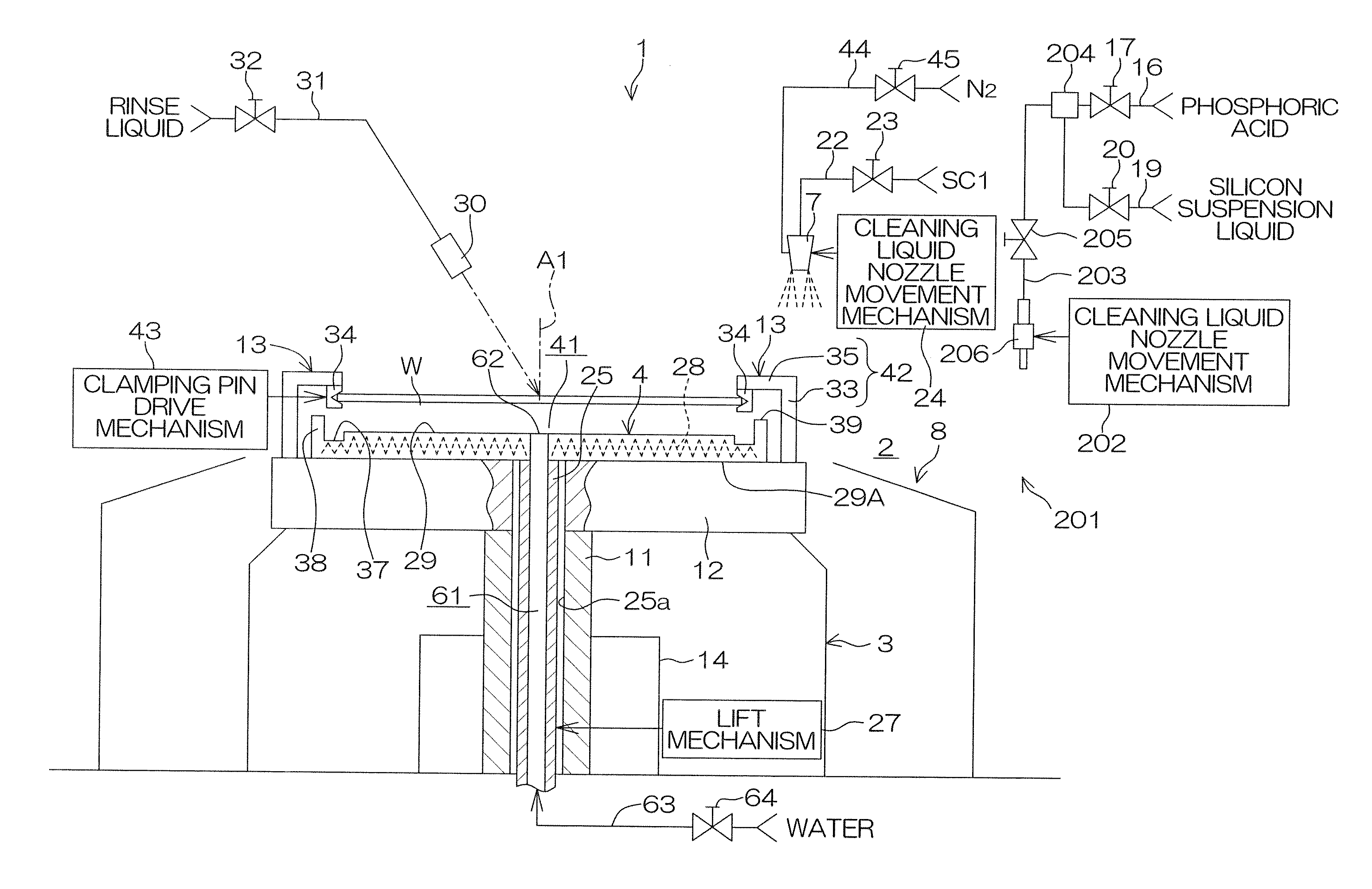
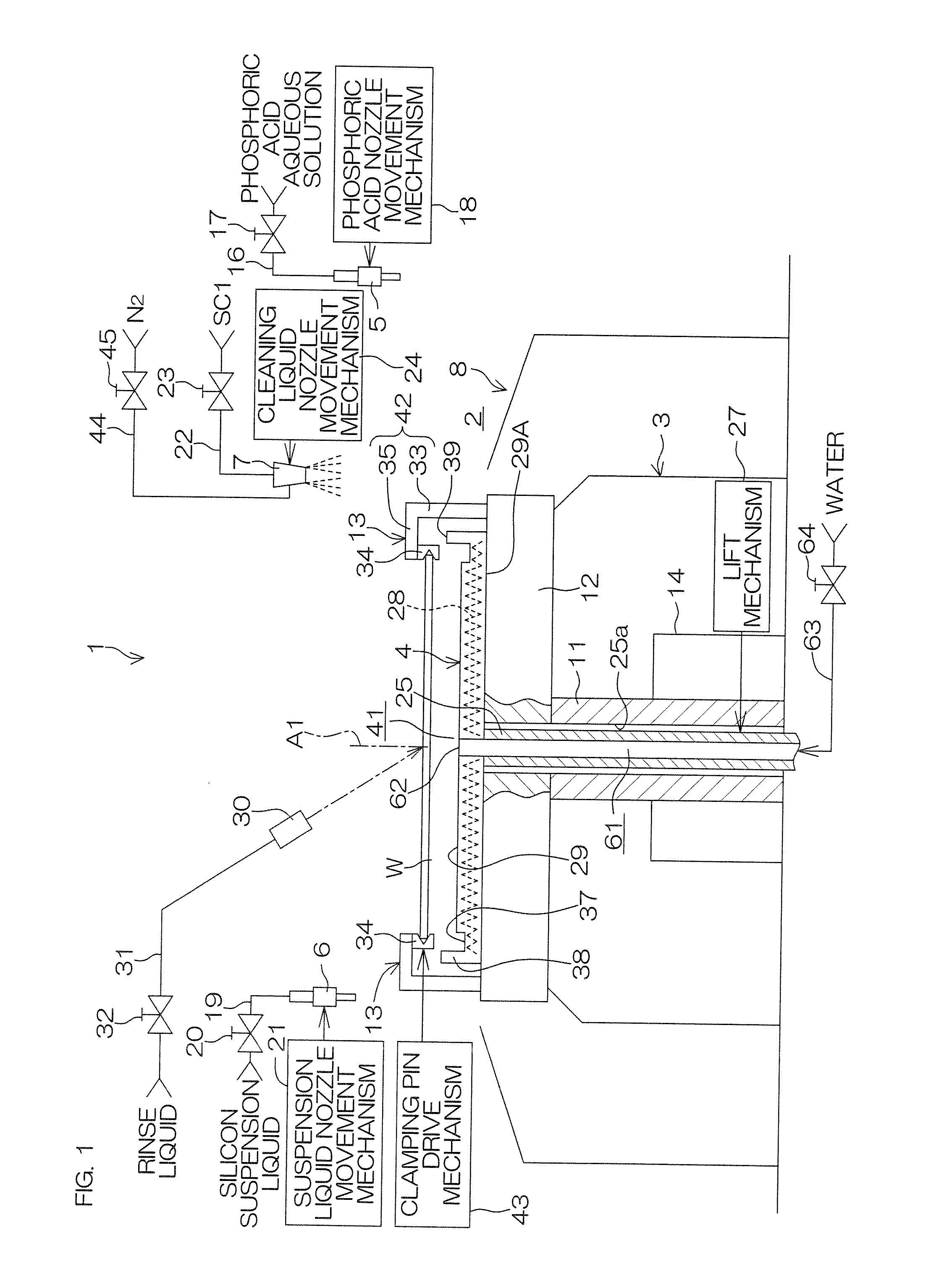
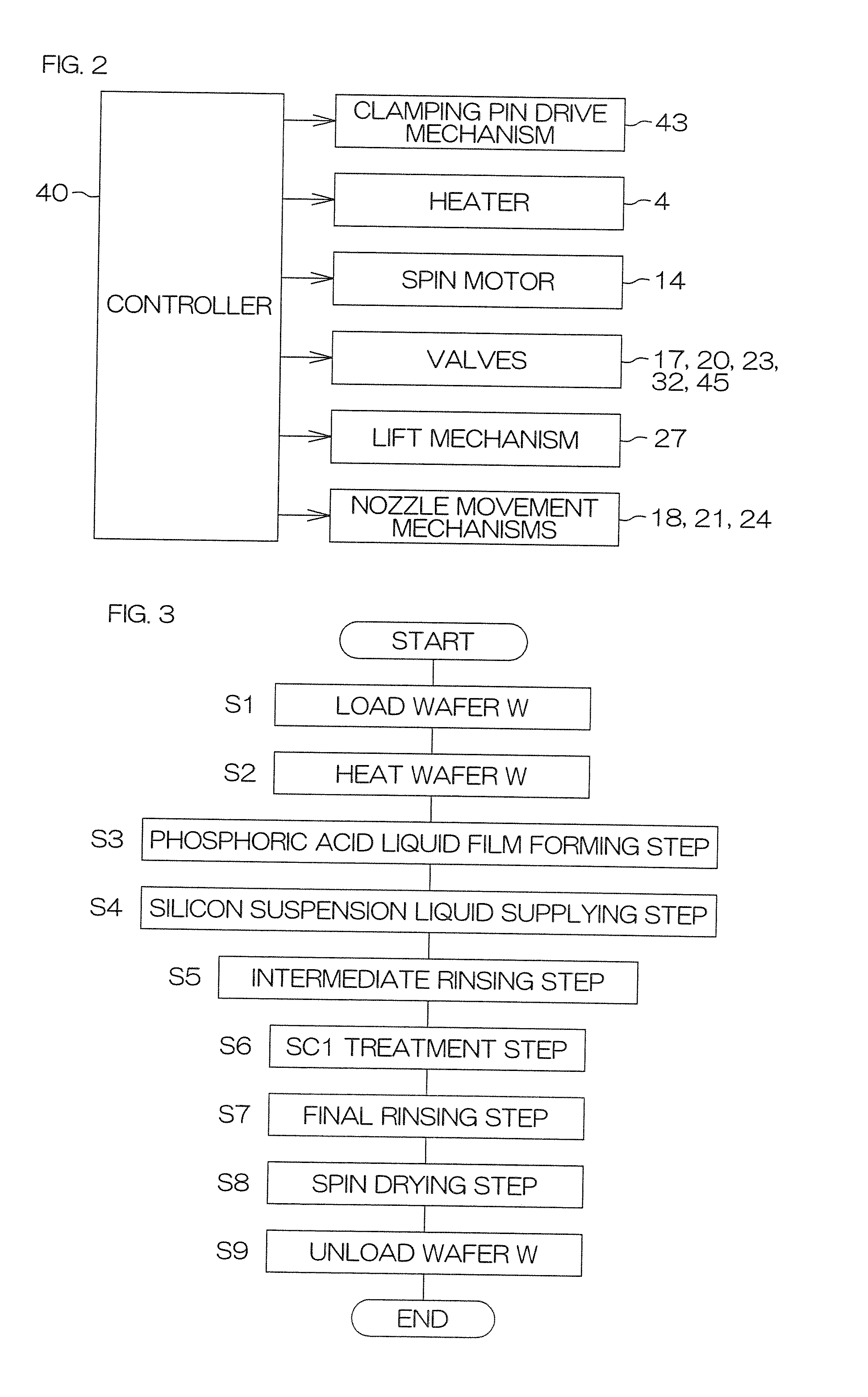
[0046]FIG. 1 is a sectional view schematically showing the construction of a substrate treatment apparatus 1 according to a first preferred embodiment of the present invention.
[0047]The substrate treatment apparatus 1 is of a single substrate treatment type adapted to perform an oxide film / nitride film etching process on a front surface (on a side including a device formation region) of a round semiconductor wafer W (an example of the substrate, hereinafter referred to simply as “wafer W”). In this etching process, both a nitride film and an oxide film are completely removed from the front surface of the wafer W, and a phosphoric acid aqueous solution is used as the etching liquid.
[0048]As shown in FIG. 1, the substrate treatment apparatus 1 includes a treatment chamber 2 defined by a partition wall (not shown), a spin chuck (substrate holding unit) 3 which horizontally holds and rotates the wafer W, a heater 4 disposed in opposed relation to a lower surface of the wafer W held by t...
PUM
 Abstract
Description
Claims
Application Information
 - R&D Engineer
- R&D Manager
- IP Professional
- Industry Leading Data Capabilities
- Powerful AI technology
- Patent DNA Extraction
Browse by: Latest US Patents, China's latest patents, Technical Efficacy Thesaurus, Application Domain, Technology Topic, Popular Technical Reports.
© 2024 PatSnap. All rights reserved.Legal|Privacy policy|Modern Slavery Act Transparency Statement|Sitemap|About US| Contact US: help@patsnap.com