Bond pad structure and method of manufacturing the same
a technology of bond pad and manufacturing method, which is applied in the manufacture of cables/conductors, metallic pattern materials, and semiconductor/solid-state device details, etc., can solve the problems of lowering the possibility of bond pad damage during the etching process and lowering manufacturing costs, so as to reduce the possibility of bond pad damage during the etching process and reduce manufacturing costs
- Summary
- Abstract
- Description
- Claims
- Application Information
AI Technical Summary
Benefits of technology
Problems solved by technology
Method used
Image
Examples
first embodiment
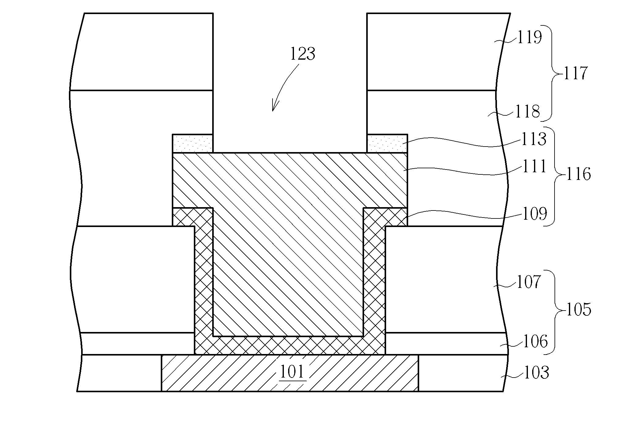
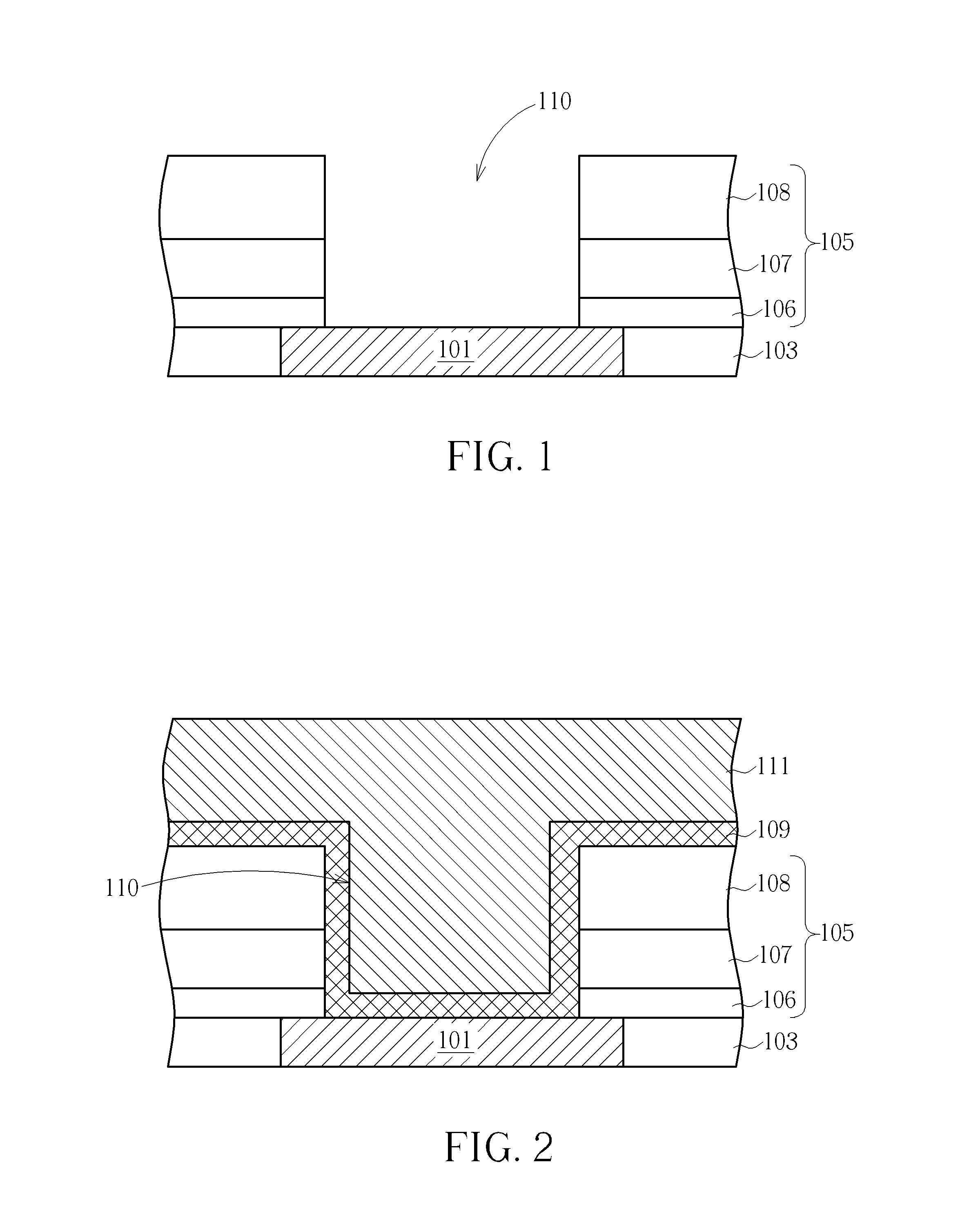
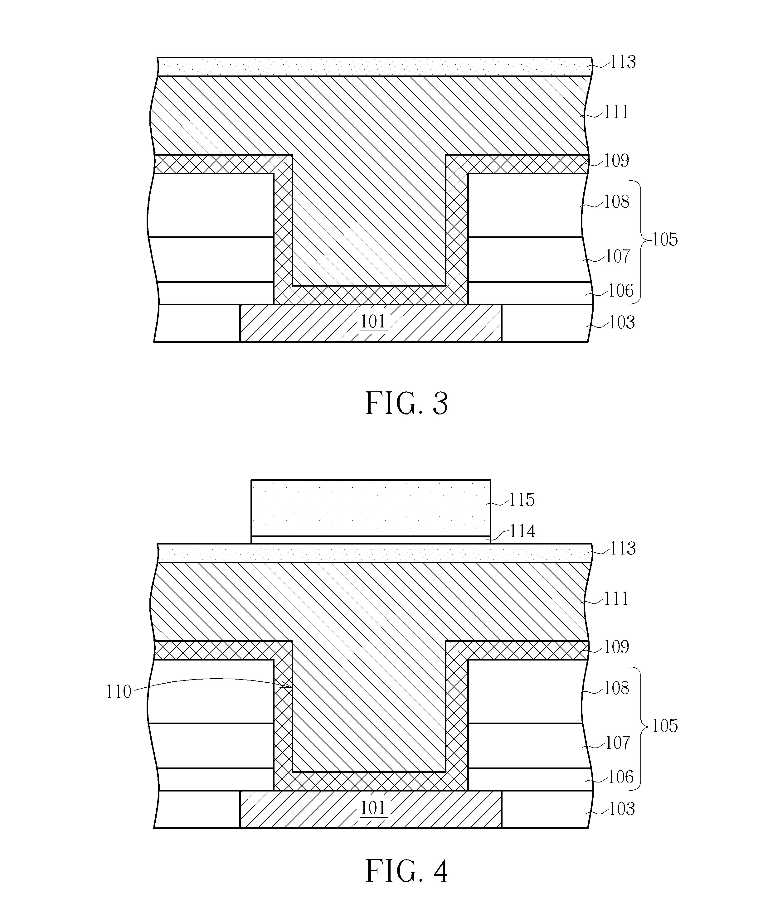
[0020]Please now refer to FIGS. 1-6, which illustrates the process flow in first embodiment of the present invention. The process of the present embodiment is particularly directed to form a protruding bond pad structure which is suitable for direct wire bonding in packaging processes.
[0021]First, the process of present embodiment starts from a prepared copper interconnection, for example: a top metal Cu layer or a Cu contact. As shown in FIG. 1, this copper structure may be a copper layer 101 deposited within a patterned opening formed in an insulating layer 103, such as a layer made of fluorinated TEOS (tetraethoxysilane) or fluorinated silicate glass (FSG). In the first place, the copper layer 101 is designed to serve as a contact for connecting the external electrical circuit. However, as mentioned in the description of the prior art, a copper interconnection may usually require an aluminum cap or pad structure to protect the copper from environmental deterioration, such as oxid...
second embodiment
[0030]Now, please refer to FIGS. 7-10 which illustrate the cross-sectional view of a process flow for manufacturing a bond pad structure with dual passivations in accordance with present invention.
[0031]The process of the present embodiment is particularly directed to form an embedded bond pad structure wherein each Al bond pad is embedded in, rather than protruding from the passivation layer. This kind of embedded bond may be suitable for processes or packaging with solder ball limiting metallurgy (BLM) or solder bumps.
[0032]As shown in FIG. 7, the present embodiment starts from a prepared pad structure similar to the bond pad 116 shown in FIG. 5, wherein the protection layer 113 is still present on the bond pad structure, and the photoresist 115 and BARC 114 used in pad etching process have already been removed. The difference between the bond pad structures shown in FIG. 5 and FIG. 7 is that the passivation layer 105 of the bond pad structure in FIG. 7 is made of only a SiN layer...
PUM
| Property | Measurement | Unit |
|---|---|---|
| corrosion | aaaaa | aaaaa |
| thick | aaaaa | aaaaa |
| size | aaaaa | aaaaa |
Abstract
Description
Claims
Application Information


