Automatic gain control electronic circuit with dual slope for an amplifier

a gain control and automatic technology, applied in the field of electronic circuits, can solve the problems of many relatively complicated electronic components, low design efficiency, and inability to easily take into account the fast gain adaptation, so as to reduce the gain of the loop, accelerate the adaptation attack time, and speed up the setting time

Active Publication Date: 2014-05-01
EM MICROELECTRONIC-MARIN
View PDF5 Cites 1 Cited by
  • Summary
  • Abstract
  • Description
  • Claims
  • Application Information

AI Technical Summary

Benefits of technology

[0017]One advantage of the electronic circuit for the automatic gain control of at least one input amplifier lies in the fact that it is very compact and provides dual slope analogue adaptation of the input amplifier gain, which gives a very fast setting time. During any transition of the input signal level, there is a dynamic, analogue increase of the gain in the automatic gain control loop to accelerate the adaptation attack time. However, the loop gain decreases towards a stable operation gain of the electronic circuit.
[0018]To perform this dual slope adaptation in the loop, at least one non-linear, analogue transconductance element is used in a non-linear amplifier-comparator. This non-linear transconductance element has a low transconductance value when the deviation of the non-linear amplifier-comparator input signals is below a determined threshold. However, this non-linear transconductance element has a high transconductance value when the non-linear amplifier-comparator input signal deviation is above a determined threshold, which defines the fast, stable, dual slope adaptation.
[0019]Advantageously, using a non-linear amplifier-comparator for the dual slope adaptation of the input amplifier gain reduces the attack time for fast gain setting in the automatic gain control loop. As a result, it is also possible to perform a fast electronic test of this type of electronic circuit at the end of the integrated circuit manufacturing method, even if the data rate in the incoming signals to be processed in the electronic circuit is low.

Problems solved by technology

However, the design of this type of electronic circuit is relatively complicated to reduce the setting time of the automatic gain control loop, which is a drawback.
Moreover, fast gain adaptation cannot easily be taken into account when the demodulator output voltage is below the first threshold level, which is another drawback.
However, to perform this adaptation in the automatic gain control loop, many relatively complicated electronic components must be used, which is a drawback.
Further, this does not facilitate the electronic testing of the electronic circuit, which is another drawback.

Method used


Image

  • Automatic gain control electronic circuit with dual slope for an amplifier
  • Automatic gain control electronic circuit with dual slope for an amplifier
  • Automatic gain control electronic circuit with dual slope for an amplifier

Examples


first embodiment

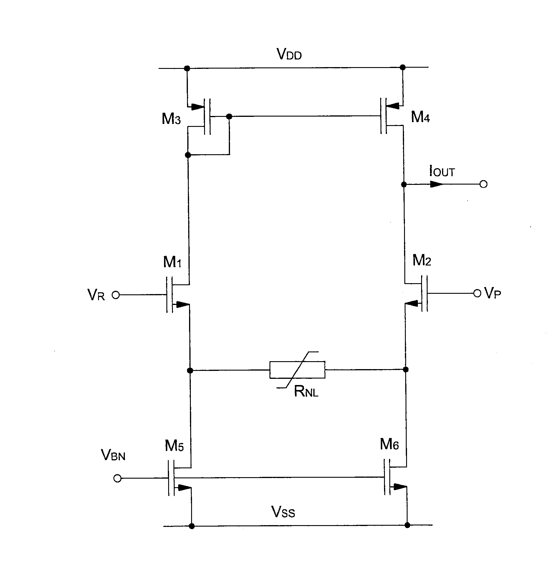
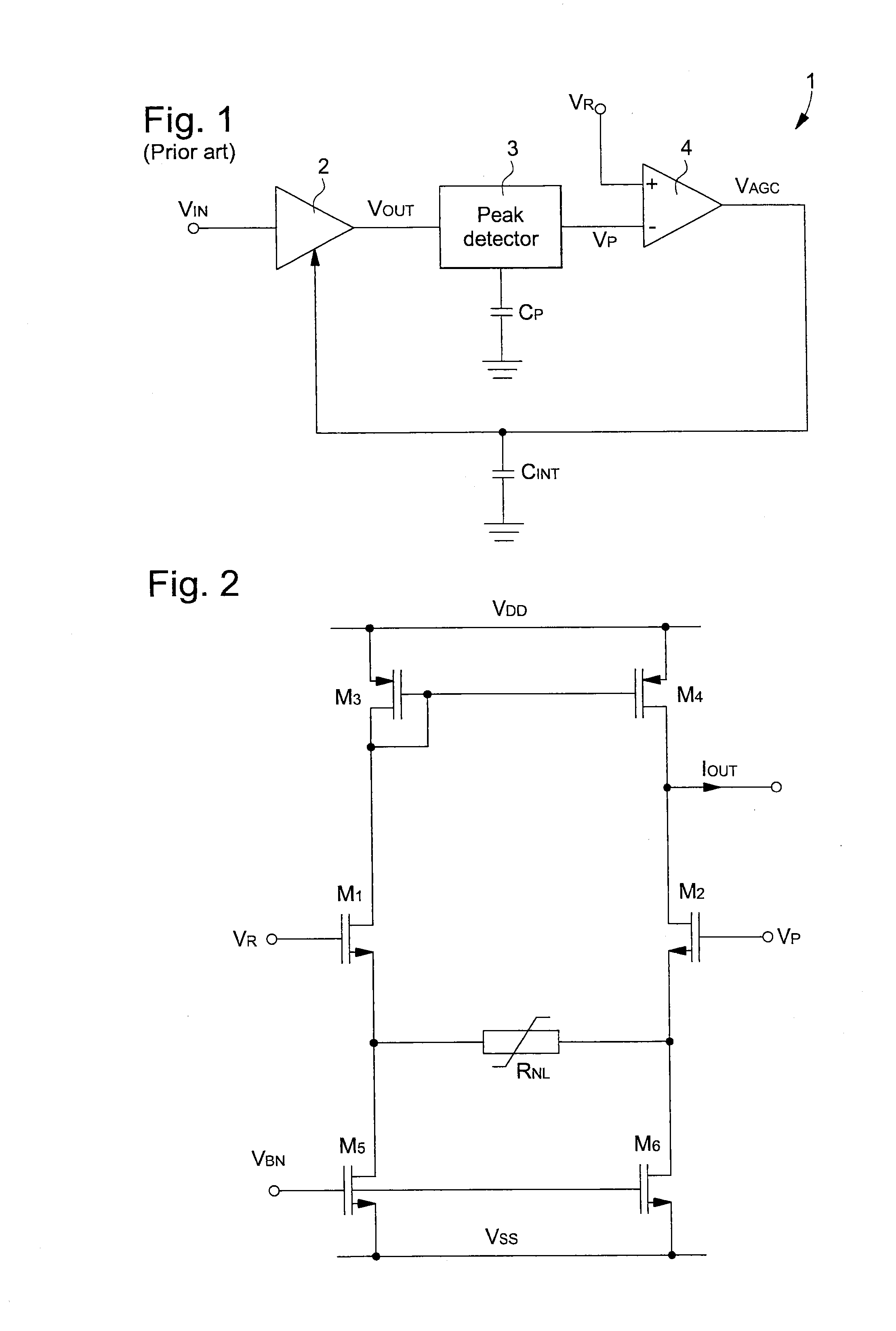
[0040]the non-linear transconductance element of the non-linear amplifier-comparator is shown in FIG. 3. It should be noted that those elements in FIG. 3 that are the same as those in FIG. 2 described above bear identical reference signs. Consequently, for the sake of simplification, the description of all these elements will not be repeated.

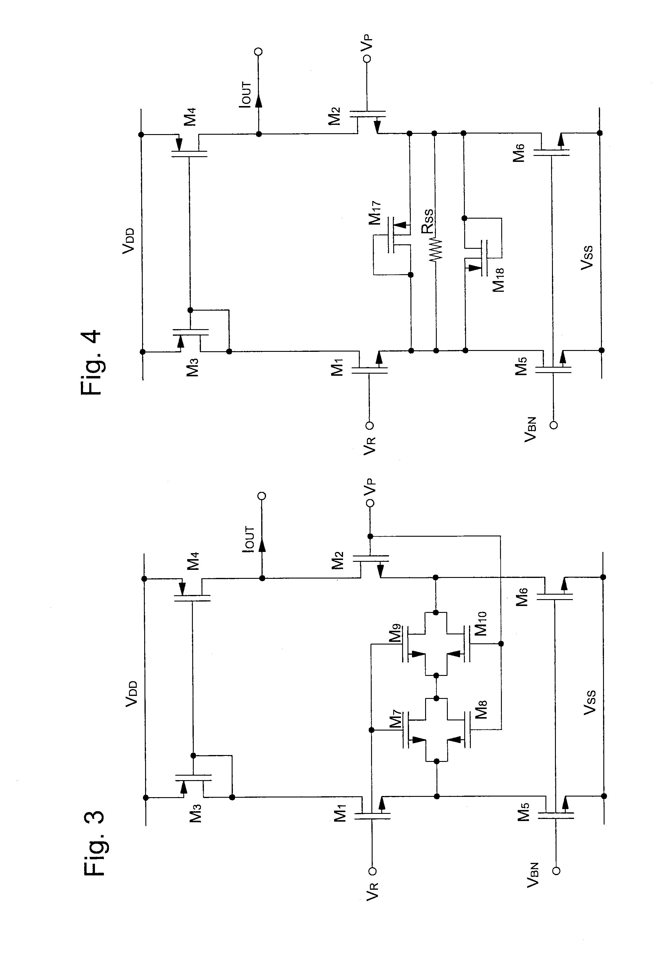
[0041]The non-linear transconductance element is formed of two pairs of transistors having a first type of conductivity M7, M8, M9 and M10 series-connected between the source or emitter of the first input transistor M1 and the source or emitter of the second input transistor M2. The sources or emitters of the two transistors M7 and M8 of the first pair are connected to the source or emitter of the first input transistor M1. The drains or collectors of the two transistors M7 and M8 of the first pair are connected to the sources or emitters of the two transistors M9 and M10 of the second pair. The drains or collectors of the two transistors M9 and...

second embodiment

[0046]the non-linear transconductance element of the non-linear amplifier-comparator is shown in FIG. 4. It should be noted that those elements in FIG. 4 which are the same as those in FIGS. 2 and 3 bear identical reference signs. Consequently, for the sake of simplification, the description of all these elements will not be repeated.

[0047]The non-linear transconductance element is formed of two diode-connected transistors M17 and M18 having a second type of conductivity and a resistance RSS all connected in parallel and connected to the sources or emitters of input transistors M1 and M2. The source or emitter of the first diode-connected transistor M17 is connected to the source or emitter of the second input transistor M2, while the gate or the base and the drain or the collector of the first diode-connected transistor M17 are connected to the source or emitter of the first input transistor M1. The source or emitter of the second diode-connected transistor M18 is connected to the ...

third embodiment

[0050]the non-linear transconductance element of the non-linear amplifier-comparator is shown in FIG. 5. It should be noted that those elements in FIG. 5 that are the same as those in FIGS. 2 to 4 bear identical reference signs. Consequently, for the sake of simplification, the description of all these elements will not be repeated.

[0051]The non-linear transconductance element is formed of a resistor RSS connected to the sources or emitters of input transistors M1 and M2, of a first adaptation transistor M13 having a first type of conductivity and of a second adaptation transistor M14 having a first type of conductivity. The source or emitter of the first transistor M13 is connected to the source or emitter of the first input transistor M1, while the drain or the collector of the first transistor M13 is connected to the drain or the collector of the second input transistor M2. The source or emitter of the second transistor M14 is connected to the source or emitter of the second inpu...


PUM


Abstract

The electronic circuit is arranged for the fast, automatic gain control of an input amplifier. It includes a non-linear amplifier-comparator for comparing a reference signal (VR) to an amplitude signal (VP) at the output of the input amplifier. The amplifier-comparator performs dual slope adaptation of the input amplifier gain according to a defined deviation threshold between the two input signals. The amplifier-comparator includes two branches each with three transistors connected in series between the terminals of a supply voltage source. First and second polarisation transistors (M5, M6) are connected to the first and second input transistors (M1, M2) controlled by the first and second input signals, which are respectively connected to a first diode-connected transistor (M3) and a second transistor (M4) of a current mirror. A non-linear transconductance element (RNL) connects the sources of the input transistors to define a dual slope gain adaptation of the non-linear amplifier-comparator.

Description

[0001]This application claims priority from European Patent Application No. 12190219.1 filed Oct. 26, 2012, the entire disclosure of which is incorporated herein by reference.FIELD OF THE INVENTION[0002]The present invention concerns an electronic circuit for the automatic gain control of an amplifier. The gain of the input amplifier of the electronic circuit is adapted in an automatic gain control loop, in particular with dual slope adaptation to increase the gain adaptation speed and to maintain the stability of the electronic circuit.BACKGROUND OF THE INVENTION[0003]In a conventional manner, particularly for the reception of data or control signals, this type of electronic circuit 1 may comprise the electronic components shown in FIG. 1 for the automatic gain control of an input amplifier 2. This input amplifier 2 is connected directly or via a shaping stage to an antenna receiving data and / or control signals (not shown). Input amplifier 2 amplifies an input signal VIN in the aut...

Claims


Application Information

Patent Timeline
Patent Type & Authority Applications(United States)
IPC IPC(8): H03G3/30
CPCH03G3/30H03F3/45197H03G3/3052
Inventor TAJALLI, ARMIN
Owner EM MICROELECTRONIC-MARIN
Why Eureka
Try Eureka