Method of forming metal gate
- Summary
- Abstract
- Description
- Claims
- Application Information
AI Technical Summary
Benefits of technology
Problems solved by technology
Method used
Image

Examples
Embodiment Construction
[0026]Reference will now be made in detail to the embodiments of the invention, examples of which are illustrated in the accompanying drawings. Wherever possible, the same reference numbers are used in the drawings and the description to refer to the same or similar elements.
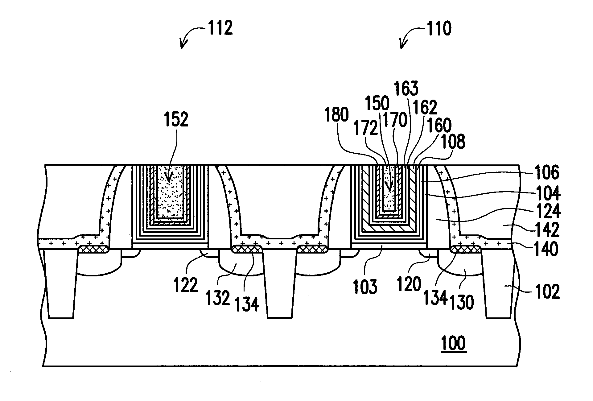
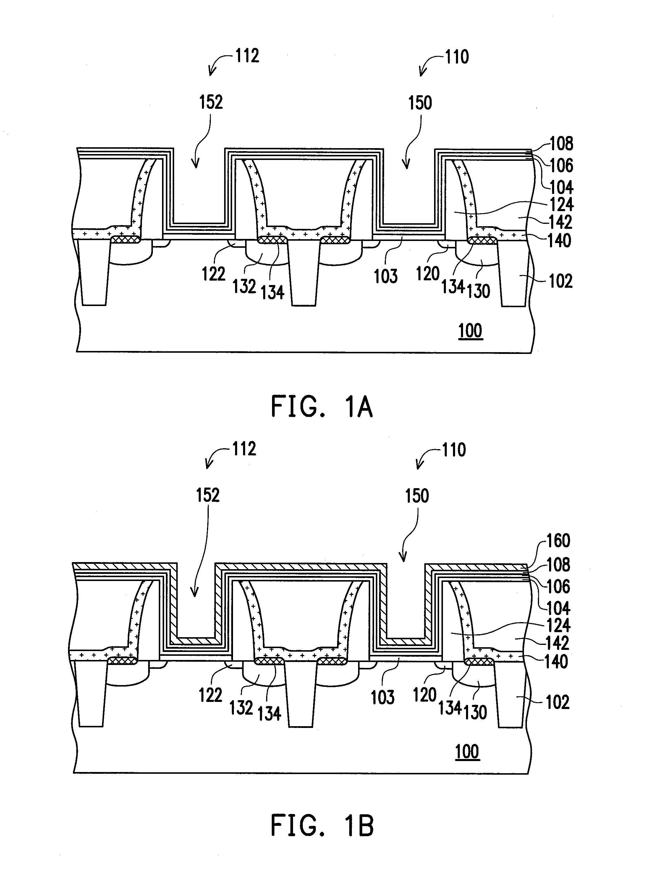
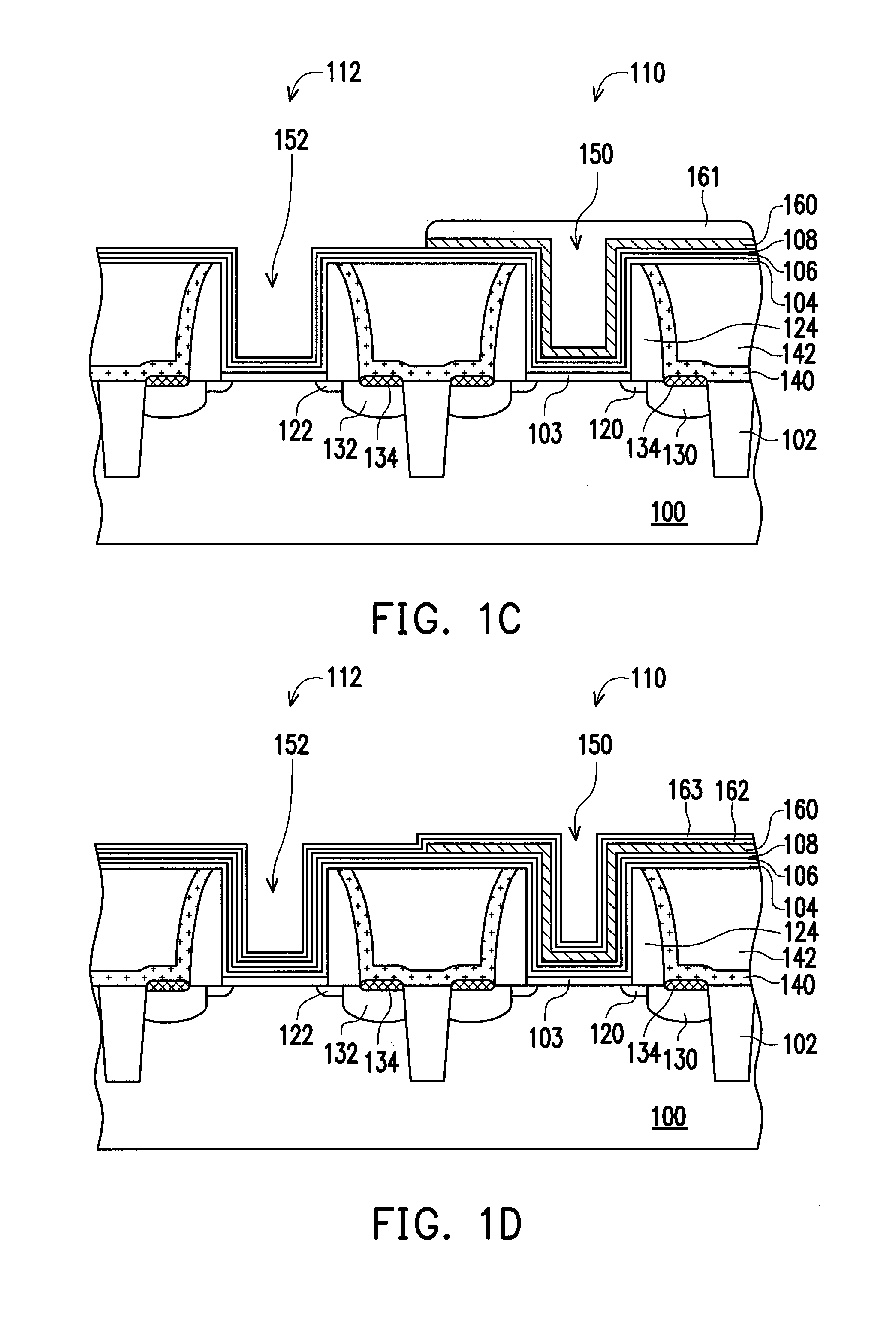
[0027]FIGS. 1A-1G are schematic cross-sectional drawings illustrating a method of forming a metal gate according to an embodiment of the present invention.
[0028]Referring to FIG. 1A, a substrate 100 such as silicon substrate, silicon-containing substrate, or silicon-on-insulator (SOI) substrate is provided. The substrate 100 has a first device region 110 and a second device region 112 formed thereon. A shallow trench isolation (STI) structure 102 is formed in the substrate 100 between the first device region 110 and the second device region 112, providing electrical isolation therebetween. In the present embodiment, a PMOS may be formed in the first device region 110 and a NMOS may be formed in the second device...
PUM
 Abstract
Description
Claims
Application Information
 - R&D Engineer
- R&D Manager
- IP Professional
- Industry Leading Data Capabilities
- Powerful AI technology
- Patent DNA Extraction
Browse by: Latest US Patents, China's latest patents, Technical Efficacy Thesaurus, Application Domain, Technology Topic.
© 2024 PatSnap. All rights reserved.Legal|Privacy policy|Modern Slavery Act Transparency Statement|Sitemap