Electroplating and electroless plating of conductive materials into openings, and structures obtained thereby

a technology of electroless plating and conductive materials, which is applied in the direction of electrical equipment, semiconductor devices, semiconductor/solid-state device details, etc., can solve the problems of void formation in the electroplated metal and does not allow the electroplating to be initiated, and achieves low tool cost and high throughput

Inactive Publication Date: 2005-05-24
INVENSAS CORP
View PDF26 Cites 129 Cited by
  • Summary
  • Abstract
  • Description
  • Claims
  • Application Information

AI Technical Summary

Benefits of technology

[0005]Metal deposition by electroplating offers the advantages of high throughput and low tool cost. Electroless plating has similar advantages. T...

Problems solved by technology

The undesirable result is formation of voids in the electroplated metal.
The edges of the dry film mask overhang the opening and do not allow the seed layer to be deposited...

Method used


Image

  • Electroplating and electroless plating of conductive materials into openings, and structures obtained thereby
  • Electroplating and electroless plating of conductive materials into openings, and structures obtained thereby
  • Electroplating and electroless plating of conductive materials into openings, and structures obtained thereby

Examples


Embodiment Construction

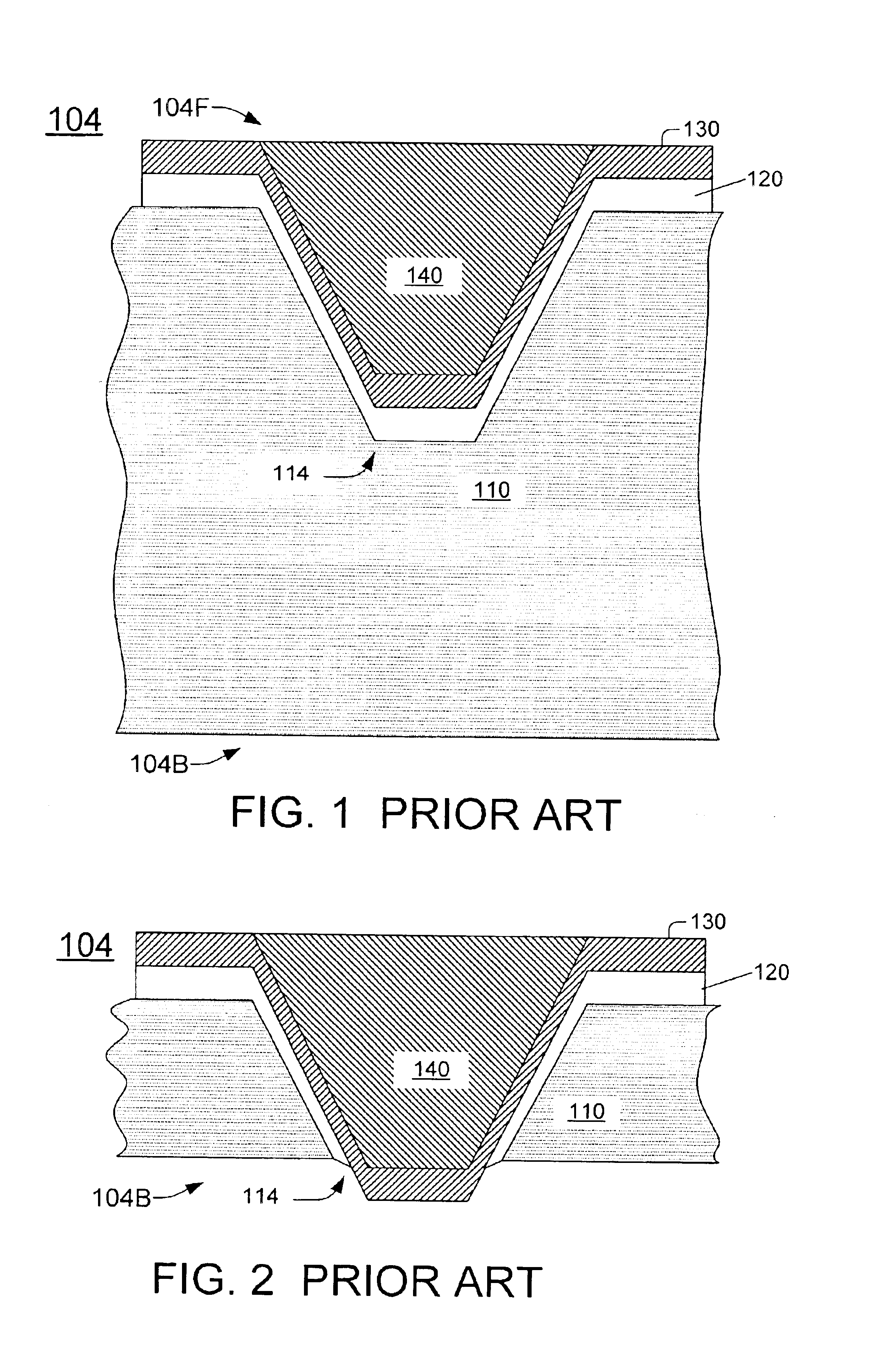
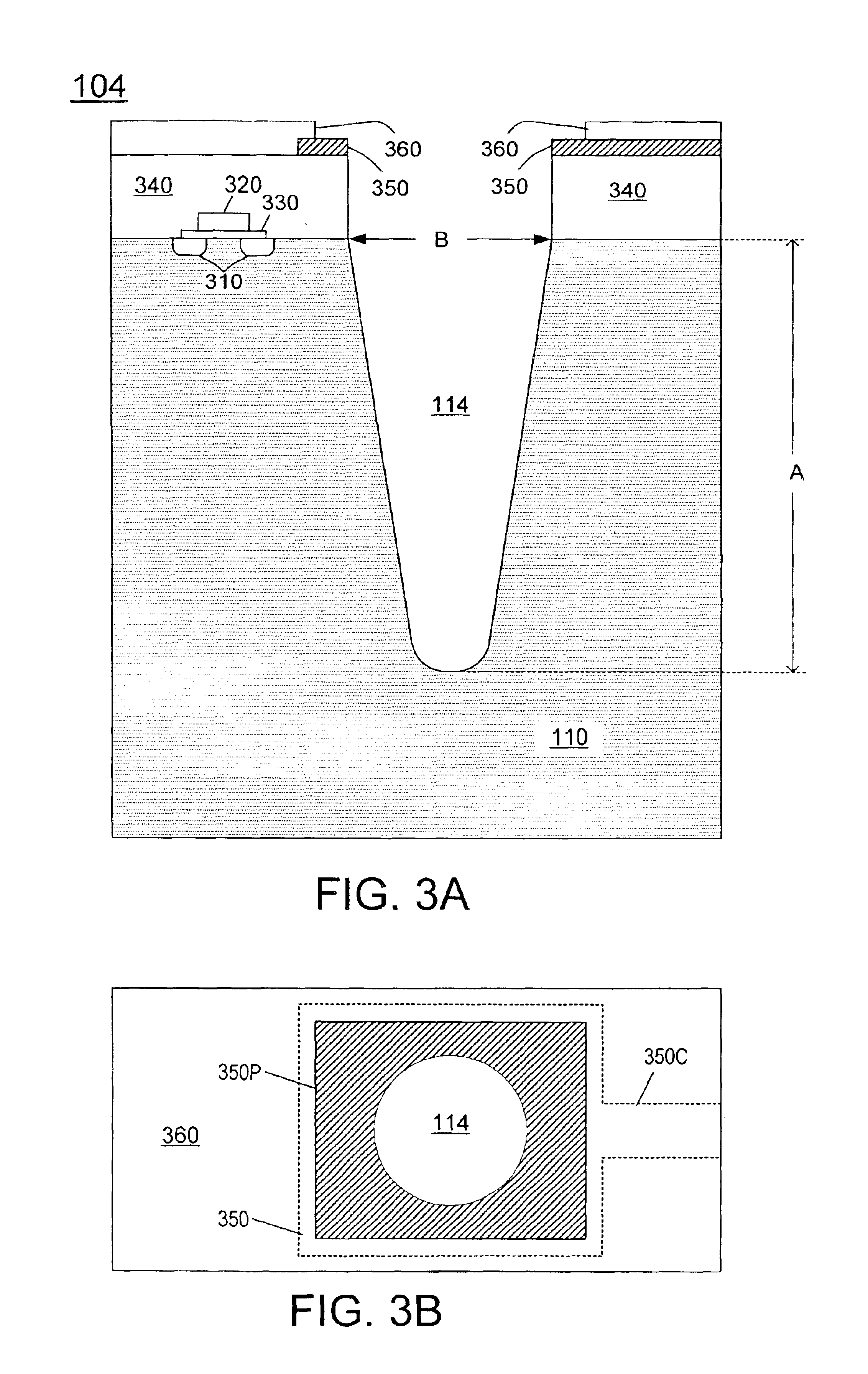
[0021]FIG. 3A illustrates a cross section of a wafer 104. The wafer includes a semiconductor substrate 110. For illustration, it will be assumed that substrate 110 is made of silicon, although other semiconductor materials can be used. The invention is not limited to any materials, dimensions, or other details, but is defined by the appended claims.

[0022]Transistors, diodes, resistors, capacitors, interconnect lines, or other devices and circuits, or portions thereof, may have been formed in wafer 104. FIG. 3A shows a MOS transistor. Its source / drain regions 310 are doped regions formed in the top surface of substrate 110. Gate 320 is formed over the channel region located between the source / drain regions. Dielectric 330 insulates the gate from the channel region. A layer 340, which includes dielectric and conductive layers, has been formed over the substrate 110 and over the transistor. Conductive layer 350 (e.g. aluminum) has been formed over the layer 340 and patterned to provide...


PUM


Abstract

A through hole (114) is formed in a wafer (104) comprising a semiconductor substrate (110). A seed layer (610) is sputtered on the bottom surface of the wafer. The seed is not deposited over the through hole's sidewalls adjacent the top surface of the wafer. A conductor (810) is electroplated into the through hole. In another embodiment, a seed is deposited into an opening in a wafer through a dry film resist mask (1110). The dry film resist overhangs the edges of the opening, so the seed is not deposited over the opening's sidewalls adjacent the top surface of the wafer. In another embodiment, a dielectric (120) is formed in an opening in a semiconductor substrate (110) by a non-conformal physical vapor deposition (PVD) process that deposits the dielectric on the sidewalls but not the bottom of the opening. A seed (610) is formed on the bottom by electroless plating. A conductor (810) is electroplated on the seed. In another embodiment, a dielectric (2910) is formed in the opening to cover the entire surface of the opening. A non-conformal layer (120) is deposited by PVD over the sidewalls but not the bottom of the opening. The dielectric (2910) is etched off the bottom with the non-conformal layer (120) as a mask. A seed (610) is formed on the bottom by electroless plating. The non-conformal layer can be formed by electroplating. It can be tantalum deposited by electroplating, then anodized. Other embodiments are also provided.

Description

BACKGROUND OF THE INVENTION[0001]The present invention relates to electroplating and electroless plating of conductive materials into openings. In some embodiments, the plated materials are used to form through hole interconnects in integrated circuits.[0002]Fabrication of through hole interconnects in integrated circuits using electroplating has been described in U.S. Pat. No. 6,184,060 issued Feb. 6, 2001 to Siniaguine, and is illustrated in FIGS. 1 and 2. Wafer 104 includes a silicon substrate 110. The wafer has a face side 104F and a back side 104B. Openings 114 are etched in substrate 110 in the face side 104F. Dielectric 120 is deposited in the openings by chemical vapor deposition (CVD) or thermal oxidation. Metal 130 is sputtered on dielectric 120. Metal 140 is electrodeposited (electroplated) to fill up the openings.[0003]Then the wafer is thinned by an etch of the back side 104B (FIG. 2). Dielectric 120 is exposed and attacked by the etch, and metal 130 becomes exposed. Th...

Claims


Application Information

Patent Timeline
IPC IPC(8): H01L21/70H01L21/768H01L23/48H01L23/532
CPCH01L21/76843H01L21/76844H01L21/76846H01L21/76855H01L21/76873H01L21/76874H01L21/76898H01L23/481Y10S438/977H01L2924/0002H01L23/53238H01L2924/00012H01L2924/00
Inventor HALAHAN, PATRICK A.KAO, SAMLAN, BOSCOSAVASTIOUK, SERGEYSINIAGUINE, OLEG
Owner INVENSAS CORP
Why Eureka
Try Eureka