Eureka AIR delivers breakthrough ideas for toughest innovation challenges, trusted by R&D personnel around the world.

Solar cell substrate, method for manufacturing same, and solar cell using same

Inactive Publication Date: 2014-05-08
POSCO
View PDF9 Cites 10 Cited by
  • Summary
  • Abstract
  • Description
  • Claims
  • Application Information

AI Technical Summary

Benefits of technology

The present invention provides a way to prevent impurities from diffusing in a semiconductor layer. This is accomplished by using a layered structure with interfaces between layers that create a diffusion barrier. Additionally, the invention improves solar cell performance by adding impurities to the semiconductor layer. This improves performance without the need for additional doping or treatments.

Problems solved by technology

Due to the influence of global warming, fuel resource depletion, environmental pollution, or the like, a traditional method of generating energy using fossil fuels is slowly reaching its limits.
In particular, although remaining quantities of petroleum predicted by experts are slightly different, the prevailing forecast is that petroleum will be depleted within a relatively short period of time.
Although certain alternative energy sources, such as hydroelectric power, have often been as touted as alternatives to fossil fuels, their uses may be limited because the hydroelectric power generation is greatly influenced by topographic factors and climatic factors.
Farther, it is also difficult to use alternative energy sources as alternatives to fossil fuels, due to the fact that alternative energy sources generate relatively small amounts of power, or have greatly limited areas of application.
However, there is a problem, in that in the manufacturing thereof, material consumption is relatively high, resulting in high manufacturing costs, since in the manufacturing of a module for the silicon-based solar cell, such a module not only passes through somewhat complicated process steps of first manufacturing an ingot from a particular material, forming the ingot into a wafer to manufacture cells and modeling the cells, but also includes using a bulk type material.
There are many obstacles to the commercialization of such a thin film, type solar cell, since it does not yet have a high degree of energy conversion efficiency, as compared to existing silicon-based solar cells, in numerous cases.
However, although a proper amount of Na may improve efficiency of a solar cell, there may be a problem in that efficiency of the solar cell may be somewhat deteriorated if Ma is excessively diffused into the CIGS layer.
A number of attempts have recently been made to use a flexible substrate instead of a glass substrate which is expensive and mass-produced, and can only be used in a standardized form.
Since such a flexible substrate has a relatively large amount of impurities in addition to Fe and the impurities diffuse into the lower electrode or the CIGS layer, there is a problem of deteriorating efficiency of the solar cell.
However, the diffusion barrier layer should be significantly reduced in thickness to meet requirements such as film-thinning and weight-lightening of the solar cell, thereby leading to a new problem that an effective diffusion preventing effect is unable to be secured in the case of the diffusion barrier layer consisting of the single layer.

Method used


Image

  • Solar cell substrate, method for manufacturing same, and solar cell using same
  • Solar cell substrate, method for manufacturing same, and solar cell using same
  • Solar cell substrate, method for manufacturing same, and solar cell using same

Examples


example 1

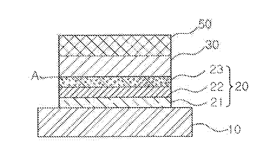
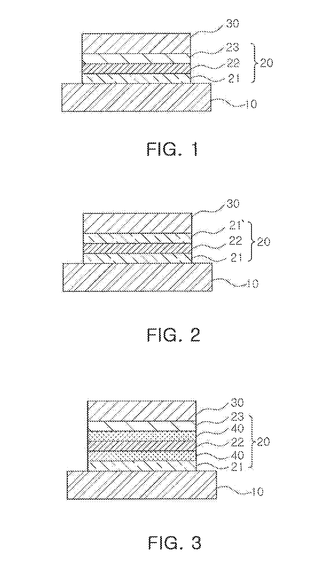
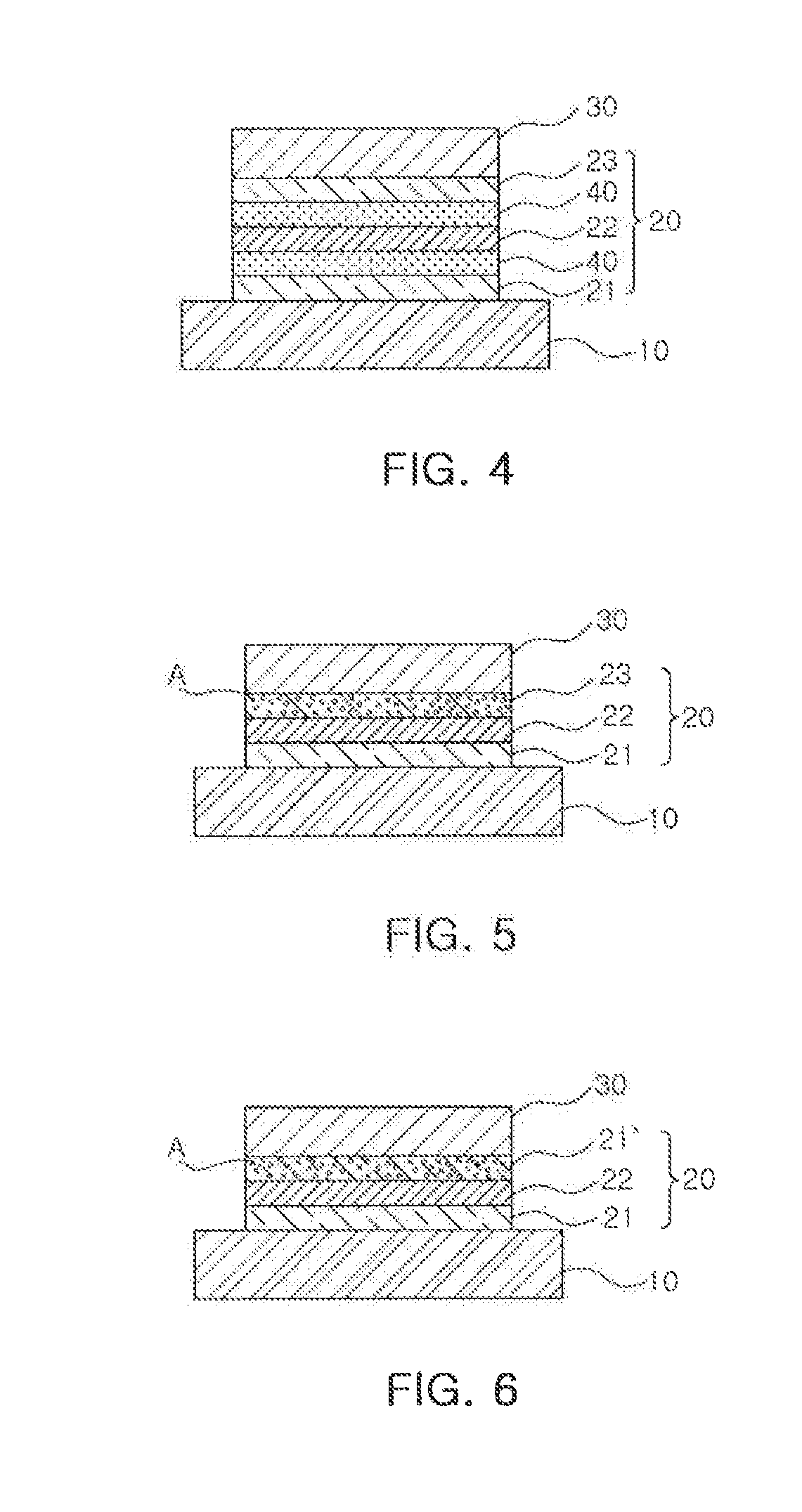
[0098]In order to check an effect of preventing diffusion of a solar cell substrate having a multilayered metal diffusion barrier layer, a stainless steel (STS 430) lower substrate was prepared, and Or was deposited on the stainless steel lower substrate to a thickness of 100 nm to form a diffusion barrier layer as Comparative Example 1. Further, Mo was deposited on the stainless steel lower substrate to a thickness of 10 nm under the same conditions as those in the Comparative Example 1, and Cr was deposited again on the deposited Mo on the stainless steel lower substrate to form a metal diffusion barrier layer formed of double layers of Mo / Cr as Inventive Example 1.

[0099]The deposition was conducted by a sputtering method, and the deposition was carried out by applying power of 1200 W to a target under conditions of a pressure of 7 mTorr and a flow rate of Ar 10 sccm.

[0100]Observation results were illustrated in FIGS. 10 and 11 respectively after heat-treating the prepared diffusi...

example 2

[0103]In order to confirm a diffusion preventing effect of a multilayered structure, a diffusion barrier layer was formed by depositing SiO2 to a thickness of 1000 nm on the stainless steel substrate using a substrate made of stainless steel (STS 430 material) as Comparative Example 2. Further, Mo was deposited on the stainless steel substrate to a thickness of 60 nm under the same conditions as those in the Comparative Example 2, and SiO2 was deposited on the deposited Mo of the stainless steel substrate to a thickness of 1000 nm to form, a diffusion barrier layer formed, of double layers of SiO2 / Mo as Inventive Example 2.

[0104]The deposition process of SiO2 was executed by a PECVD method, wherein the SiO2 was deposited, by applying a power of 200 W and maintaining flow rates of N2O 600 sccm, SiH4 45 sccm and Ar 700 sccm under a pressure of 800 mTorr. The Mo was deposited by applying a power of 1200 W and maintaining a flow rate of Ar 10 sccm under a pressure of 7 mTorr.

[0105]Obser...

example 3

[0108]In order to confirm a diffusion preventing effect of a multilayered structure including an oxide layer, photo-conversion efficiency of a solar cell according to whether the oxide layer had been formed or not was measured. An ordinary sodalime glass substrate was applied in Comparative Example 3. A diffusion barrier layer was formed in Comparative Example 4 by preparing a substrate made of stainless steel (STS 430 material) and depositing SiO2 to a thickness of 1000 nm on the stainless steel substrate. Further, a diffusion barrier layer consisting of double layers of SiO2 / Mo was formed in Inventive Example 3 by depositing Mo so a thickness of 20 nm on a stainless steel substrate under the same conditions as those in the above-mentioned stainless steel substrates and depositing SiO2 to a thickness of 500 nm on the deposited Mo of the stainless steel substrate. In addition, a diffusion barrier layer consisting of quadruple layers of SiO2 / Mo / SiO2 / Mo was formed in Inventive Example...


PUM

PropertyMeasurementUnit
Temperatureaaaaaaaaaa
Fractionaaaaaaaaaa
Percent by massaaaaaaaaaa

Abstract

One aspect of the present invention is a solar cell substrate, comprising: a lower substrate; and a lower electrode that is formed on the upper part of said lower substrate, wherein a metal diffusion-preventing film having at least one or two or more metal layers is included between said lower substrate and said lower electrode, and if two or more metal layers are formed, the metal layers adjoining each other can be different metals. Additionally, a solar cell, which is another aspect of the present invention, comprises: a lower substrate; and a lower electrode that is formed on the upper part of said lower substrate, wherein a metal diffusion-preventing film having at least one or two or more metal layers is included between said lower substrate and said lower electrode, and if two or more metal layers are formed, the metal layers adjoining each other comprise solar cell substrates which are of different metals; p-type light absorption layers formed on said solar cell substrates; n-type buffer layers formed on said light absorption layers; transparent windows formed on said buffer layers; and upper electrodes formed on said transparent windows.

Description

TECHNICAL FIELD[0001]The present invention relates to a CI(G)S solar cell substrate, a method for manufacturing the solar cell substrate, and a solar cell including the solar cell substrate.BACKGROUND ART[0002]Due to the influence of global warming, fuel resource depletion, environmental pollution, or the like, a traditional method of generating energy using fossil fuels is slowly reaching its limits. In particular, although remaining quantities of petroleum predicted by experts are slightly different, the prevailing forecast is that petroleum will be depleted within a relatively short period of time.[0003]Further, according to the convention on energy use and climate change, represented by the Kyoto Protocol, it is compulsorily required that the generation of carbon dioxide produced by the combustion of fossil fuels should be decreased. Therefore, it is clear that the continued use of fossil fuels will have effect on all countries in the world, as well as current treaty powers, so ...

Claims


Application Information

Patent Timeline
IPC IPC(8): H01L31/0216H01L31/18
CPCH01L31/18H01L31/02167H01L31/03928H01L31/0749Y02E10/541Y02P70/50
Inventor KIM, KYOUNG-BOPARK, YOUNG-JUNBAEK, JE-HOONKIM, JONG-SANGKIM, YOUNG-GEUN
Owner POSCO
Why Eureka
Eureka Blog
Learn More