Methods and systems for humidity and pressure sensor overlay integration with electronics

a humidity sensor and electronic technology, applied in the field of sensors, can solve the problems of difficult to gear toward general applications, and difficult to achieve the effect of general application of mems fabrication processes, and achieve the effect of reducing the cost of system footprint, reducing the cost of system components, and improving the performance of devices

Active Publication Date: 2014-05-08
MEMS VISION INT
View PDF4 Cites 38 Cited by
  • Summary
  • Abstract
  • Description
  • Claims
  • Application Information

AI Technical Summary

Benefits of technology

[0014]In accordance with an embodiment of the invention there is provided a method comprising providing a capacitive based sensor over a first predetermined portion of a wafer comprising at least a first ceramic element providing protection for the final capacitive based sensor and self-aligned processing during its manufa...

Problems solved by technology

In addition, this integration can bring forward enhanced performance through the optimal interconnection with signal processing electronics or added functionality through the inclusion of many sensing devices, with marginal cost of system footprint.
However, because of this vast range of functionality, MEMS fabrication processes, unlike the microelectronics industry, are difficult to gear towards general applications.
As a result, most processes historically have been aimed at the fabrication of a few specific device types, and usually performance of the devices is hindered by process variability.
This is essentially because of the unparalleled benefits available from CMOS in the areas of circuit size, operating speed, energy efficiency and manufacturing costs which continue to improve from the geometric downsizing that comes with every new generation of semiconductor manufacturing processes.
This power consumption arising from the charging and discharging of various load capacitances within the CMOS gates, mostly gate and wire capacitance, but also transistor drain and transistor source capacitances, whenever they are switched.
However, combining CMOS and MEMS technologies has been especially challenging because some MEMS process steps—such as the use of special m...

Method used


Image

  • Methods and systems for humidity and pressure sensor overlay integration with electronics
  • Methods and systems for humidity and pressure sensor overlay integration with electronics
  • Methods and systems for humidity and pressure sensor overlay integration with electronics

Examples


Embodiment Construction

[0040]The present invention is directed to humidity sensors and more particularly MEMS based capacitive sensors which may be manufactured directly over silicon based CMOS electronics.

[0041]The ensuing description provides exemplary embodiment(s) only, and is not intended to limit the scope, applicability or configuration of the disclosure. Rather, the ensuing description of the exemplary embodiment(s) will provide those skilled in the art with an enabling description for implementing an exemplary embodiment. It being understood that various changes may be made in the function and arrangement of elements without departing from the spirit and scope as set forth in the appended claims.

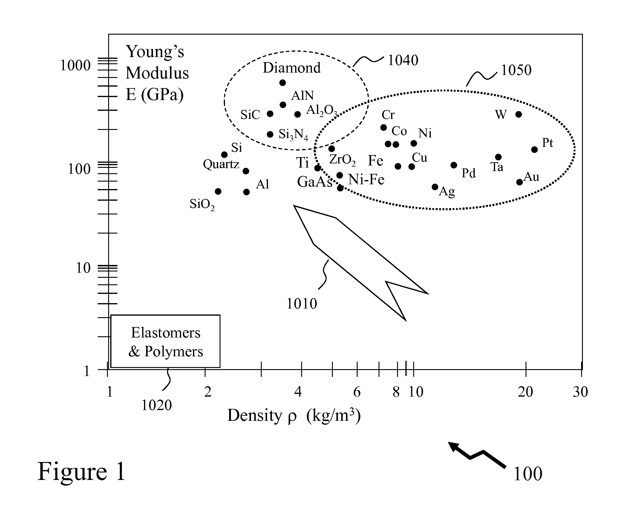
[0042]Referring to FIG. 1 shown is a material selection chart 100 for MEMS device implementations. Plotted onto the material selection chart 100 are a range of different materials including metals, dielectrics, ceramics and polymers wherein each material is represented by a point on the X—Y graph wherein ...


PUM


Abstract

Capacitive sensors and MEMS elements that can be implemented directly above silicon CMOS electronics are disclosed. A capacitive based sensor is disposed over a first predetermined portion of a wafer that includes at least a first ceramic element providing protection for the final capacitive based sensor and self-aligned processing during its manufacturing.

Description

CROSS-REFERENCE TO RELATED APPLICATIONS[0001]This patent application claims the benefit of U.S. Provisional Patent Application 61 / 719,555 filed on Oct. 29, 2012 entitled “Methods and Systems for Humidity Sensor Overlay Integration with Electronics” and U.S. Provisional Patent Application 61 / 719,558 filed on Oct. 29, 2012 entitled “Methods and Systems for Humidity and Pressure Sensor Overlay Integration with Electronics.”FIELD OF THE INVENTION[0002]The present invention relates to sensors and more particularly MEMS based capacitive sensors and capacitive humidity sensors which may be manufactured directly over silicon based CMOS electronics.BACKGROUND OF THE INVENTION[0003]Sensors are transducers or converters that measure a physical quantity and convert it into a signal which can be read. Typically, that reading is by an electronic instrument which converts the signal to a measurement based upon the sensitivity of the sensor, its calibration data, and other corrections. Included wit...

Claims


Application Information

Patent Timeline
IPC IPC(8): G01N27/22
CPCG01N27/223G01L9/12G01L19/0092
Inventor EL-GAMAL, MOURADCICEK, PAUL-VAHENABKI, FREDERIC
Owner MEMS VISION INT
Why Eureka
Try Eureka