Epitaxial group III nitride layer on (001)-oriented group IV semiconductor

a technology of iii nitride and semiconductor, applied in semiconductor devices, basic electric elements, electric devices, etc., can solve the problem of difficult growth of hexadic group iii nitrides on four-fold si(001)

Inactive Publication Date: 2011-05-03
AZZURRO SEMICON
View PDF1 Cites 3 Cited by
  • Summary
  • Abstract
  • Description
  • Claims
  • Application Information

AI Technical Summary

Benefits of technology

[0014]An extremely important example of a (001) surface of a group IV semiconductor is Si(001). Here, in an exemplary embodiment, the method enables the growth of an epitaxial group III nitride layer on Si(001) with relatively small misorientations and thus the growth of epitaxial group III nitride layers on the industrially customary standard material used in integrated semiconductor electronics.
[0015]Furthermore, in one exemplary embodiment of the method according to the invention, it is possible to achieve a higher crystal quality for epitaxial group III nitride layers on misoriented (vicinal) Si(001). However, the method is also suitable for Ge surfaces, SiGe surfaces, SiGeC surfaces or other group IV surfaces.
[0018]In this exemplary embodiment, a surface reconstruction with dimers along a preferred direction is achieved, and thus a surface symmetry break which allows monocrystalline group III nitride growth.
[0020]In a further exemplary embodiment, the step of providing the substrate comprises depositing a group IV semiconductor layer of the type Si1-x-yGexCy, with x+y<1 and a strain relative to the group IV semiconductor substrate of an amount greater than 0.02%, on a group IV semiconductor substrate. By pretensioning the substrate surface by means of strained layers, it is possible, for example, depending on the strain sign, to select one of the two possible orientations of the group III nitride on the surface, which offers advantages in the case of laterally emitting optoelectronic components and also in the case of singulation of components due to the different choice of possible preferential break direction.
[0023]Additional strain, brought about for example by alloying Si with Ge or C, further improves orientation selection and reduces the twist of the grown group III nitride layer.
[0028]In one exemplary embodiment, the target temperature amounts to 1100° C., and temperature increases of 10 K / s are preferably used. In this way, a steep temperature gradient is obtained, which is also supported by the limited heat conductivity of the Si substrate. Such a temperature gradient leads throughout the Si crystal to strains and as a rule to severe tensile strain at the surface. This leads in turn, even in the case of exactly oriented substrates, to uniform surface reconstruction, which enables monocrystalline growth of group III nitrides.

Problems solved by technology

Growth of the hexadic group III nitrides on four-fold Si(001) is difficult, however, due to the unmatched symmetry.

Method used


Image

  • Epitaxial group III nitride layer on (001)-oriented group IV semiconductor
  • Epitaxial group III nitride layer on (001)-oriented group IV semiconductor
  • Epitaxial group III nitride layer on (001)-oriented group IV semiconductor

Examples


Embodiment Construction

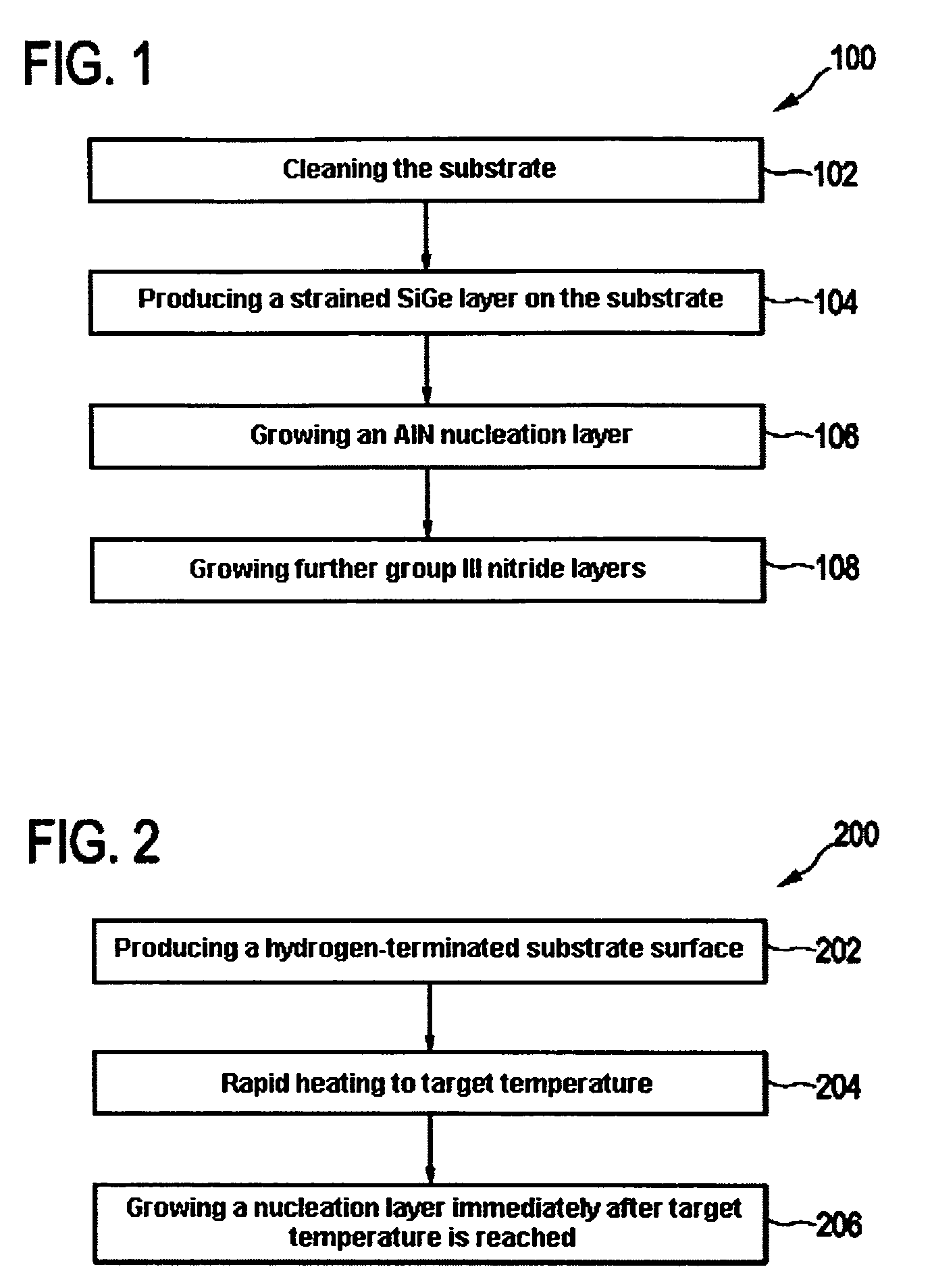
[0068]The growth of strained layers in the system of group IV elements (in particular Si, Ge, C) is most readily possible with SiGe on Si. FIG. 1 shows a flow chart of an exemplary embodiment of a method 100 for producing an epitaxial group III nitride layer on an Si(001) surface.

[0069]Such a process is started, if it is to take place in the same growth chamber as for group III nitride growth, by firstly cleaning an Si(001) substrate at temperatures of over 1000° C. in a hydrogen atmosphere (step 102). Alternatively, wet chemical cleaning may be carried out beforehand, as described in [Grundmann] for example.

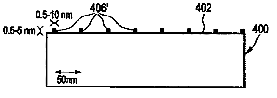
[0070]Then a strained SiGe layer is produced at temperatures preferably of around 1000° C.-1400° C., by growing a thin layer on an Si substrate with the gases present in part as dopants, such as for example SiH4 or GeH4 or indeed other gaseous or organometallic compounds of these starting materials (step 104). Sufficient for this purpose is a layer thickness of a few monolayers ...


PUM


Abstract

Group III nitride layers have a wide range of uses in electronics and optoelectronics. Such layers are generally grown on substrates such as sapphire, SiC and recently Si(111). For the purpose inter alia of integration with Si-CMOS electronics, growth on Si(001) is indicated, which is possible only with difficulty because of the different symmetries and is currently limited solely to misoriented Si(001) substrates, which restricts the range of use. In addition, the layer quality is not at present equal to that produced on Si(111) material. Growth on exactly oriented Si(001) and an improvement in material quality can now be simply achieved by a modification of the surface structure possible with a plurality of methods.

Description

CROSS REFERENCE TO RELATED APPLICATION[0001]Reference is made to and priority claimed from U.S. provisional application Ser. No. 60 / 861,672, filed Nov. 28, 2006, entitled Epitaxial group III nitride layer on (001)-oriented group IV semiconductor.BACKGROUND OF THE INVENTION[0002]1. Technical Field[0003]The invention relates to a multilayer structure with an epitaxial group III nitride layer on either a (001) surface of a group IV semiconductor or a surface of the group IV semiconductor which has a misorientation of less than 8 degrees relative to a (001) orientation. The invention further relates to a semiconductor component with such a multilayer structure and to use of a substrate with either a (001) surface of a group IV semiconductor or a surface of the group IV semiconductor which has a misorientation of less than 8 degrees relative to a (001) orientation to produce at least one epitaxial group III nitride layer thereon. Finally, the invention relates to a method of producing a ...

Claims


Application Information

Patent Timeline
Patent Type & Authority Patents(United States)
IPC IPC(8): H01L31/036
CPCH01L21/02381H01L21/0243H01L21/02433H01L21/02447H01L21/02458H01L21/0254H01L21/0262H01L21/0245H01L21/8258
Inventor SCHULZE, FABIANDADGAR, ARMINKROST, ALOIS
Owner AZZURRO SEMICON
Why Eureka
Try Eureka