Using millisecond pulsed laser welding in MEMS packaging

a technology of microelectromechanical system and laser welding, which is applied in the association of printed circuit non-printed electric components, instruments, and semiconductor/solid-state device details, etc., can solve problems such as thermal mismatch, and achieve the effect of low repetition rate and low distortion

Active Publication Date: 2014-05-08
RGT UNIV OF CALIFORNIA
View PDF10 Cites 28 Cited by
  • Summary
  • Abstract
  • Description
  • Claims
  • Application Information

AI Technical Summary

Benefits of technology

[0012]Laser welding in the present invention refers to the low repetition rate regime in which significant re-solidification of work piece occurs between laser pulses. Pulsed laser welding offers the advantage of very local heat input to the weld, resulting in low distortion and the ability to package the heat sensitive electronic components in device and wafer level.

Problems solved by technology

The cap is directly micro-welded to the substrate, therefore the thermal mismatch issue, which is the common problem for current packaging methods, is not be considered in the proposed packaging method.

Method used


Image

  • Using millisecond pulsed laser welding in MEMS packaging
  • Using millisecond pulsed laser welding in MEMS packaging
  • Using millisecond pulsed laser welding in MEMS packaging

Examples


Embodiment Construction

[0032]In the following description of the preferred embodiment, reference is made to the accompanying drawings which form a part hereof, and in which is shown by way of illustration one or more specific embodiments in which the invention may be practiced. It is to be understood that other embodiments may be utilized and structural changes may be made without departing from the scope of the present invention.

Physics of Laser Welding

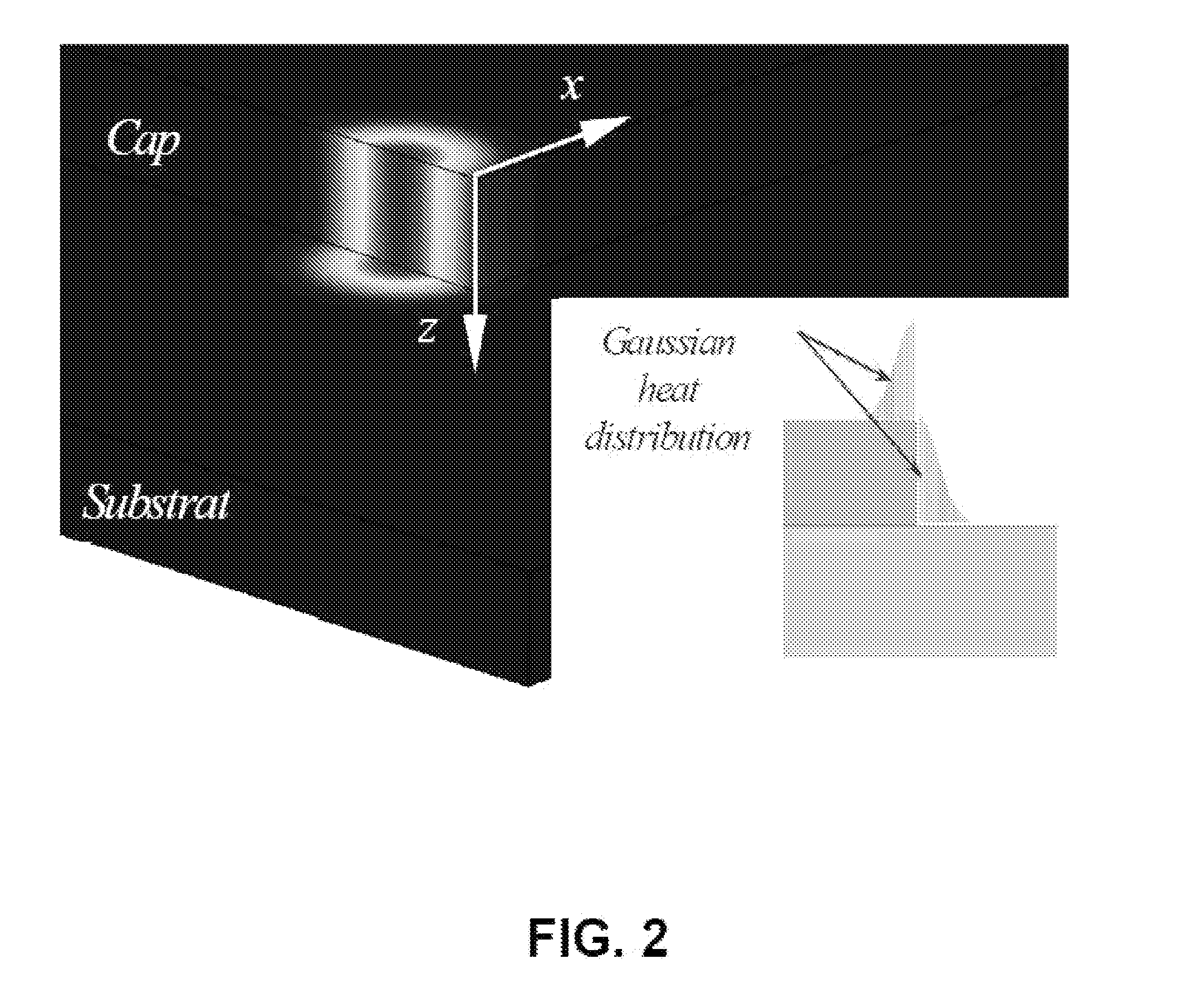
[0033]There have been several numerical and analytical models that have sought to elucidate the physical mechanisms involved in the continuous-wave laser welding process [6-8], but only a few models of pulsed laser welding exist [9]. In order to construct an adequate model of heat flow in pulsed laser welding, it is necessary to understand the physics of the laser welding process.

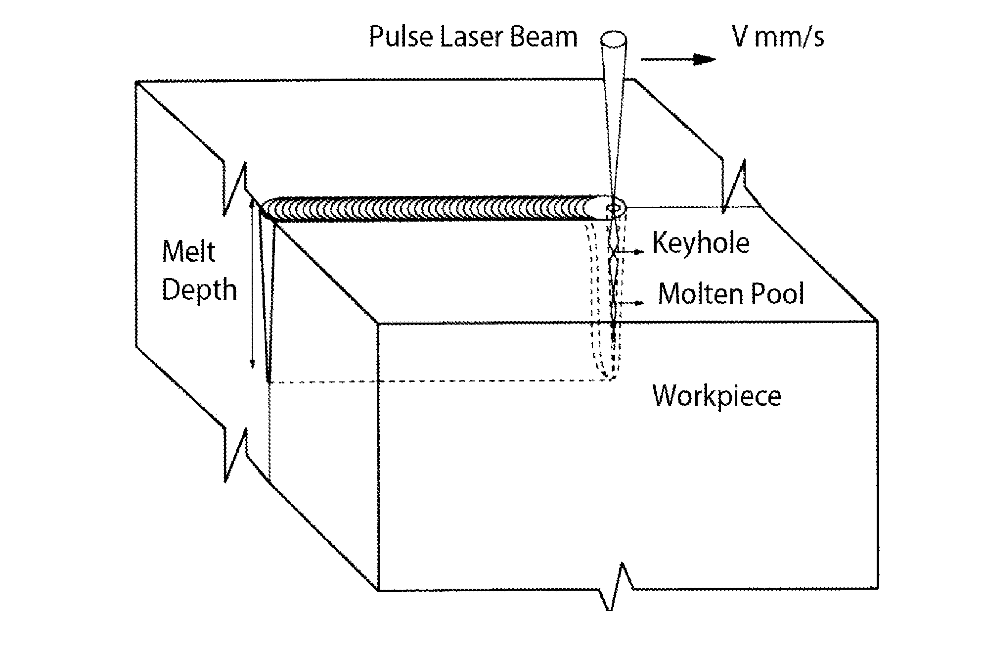
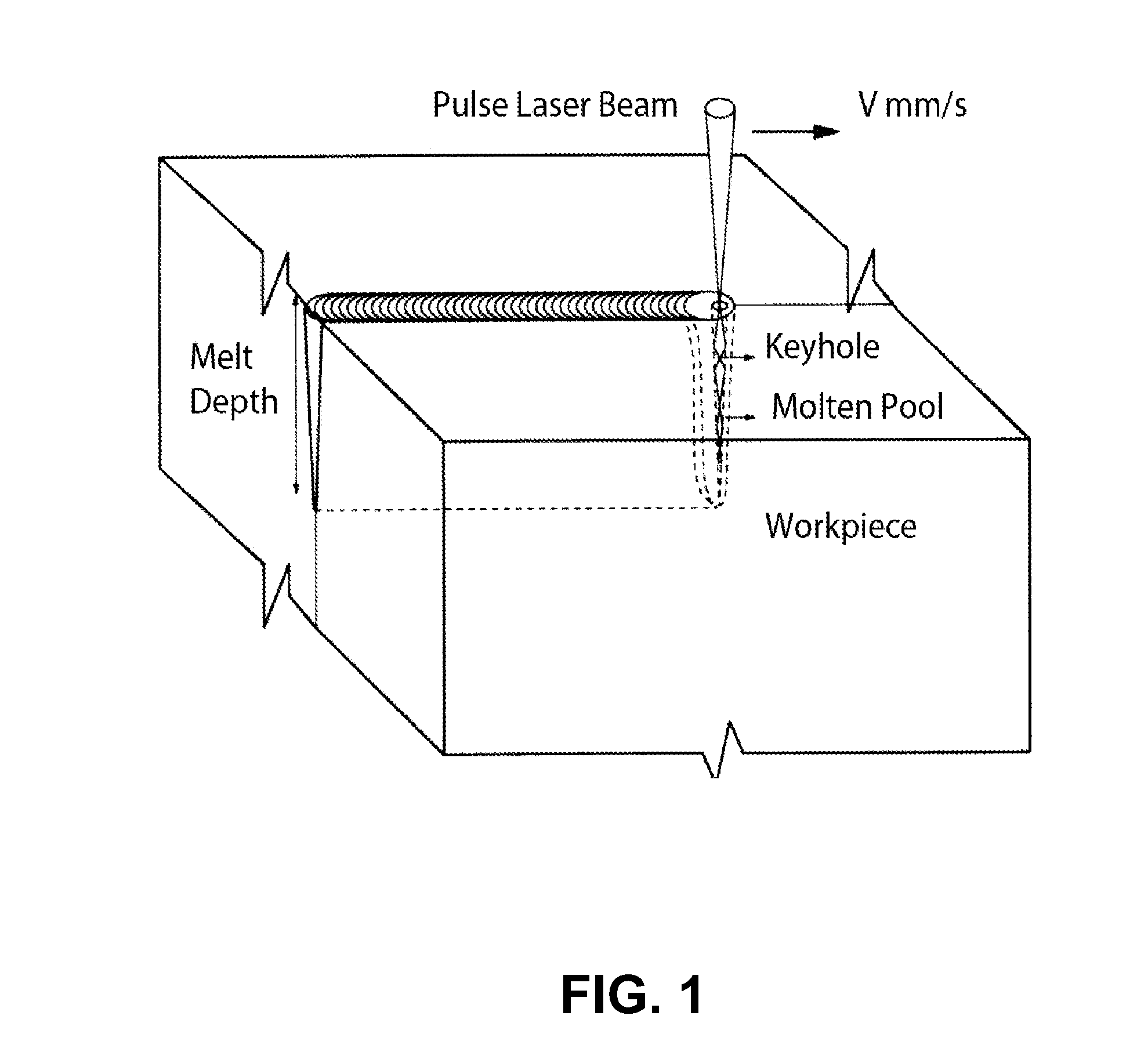
[0034]As shown in FIG. 1, when a laser beam is irradiated onto the surface of a material, the absorbed energy causes heating, melting and evaporation of the material depending on ...


PUM

PropertyMeasurementUnit
wavelengthaaaaaaaaaa
sizeaaaaaaaaaa
diameteraaaaaaaaaa

Abstract

A new packaging method for a wide range of MEMS for application on both the wafer and device scale. Titanium is used as the packaging material and both silicon and titanium MEMS devices are integrated on to a titanium substrate. A Nd:YAG pulsed laser is used to micro-weld the titanium cap to the substrate. A three-dimensional time dependent model of heat flow during laser beam welding is presented. The heat transfer and parametric design capabilities of COMSOL were employed for this purpose. Model calculations are compared and calibrated with experimental results of pulsed laser welds. The functionality and hermiticity of the proposed packaging was evaluated by packaging a self actuated Veeco Instrument AFM cantilever tip. The experimental measurements show that the resonance frequency and quality factor of the device stay the same before and after packaging and the applied technique has no effect on the device.

Description

CROSS-REFERENCE TO RELATED APPLICATIONS[0001]This application claims the benefit under 35 U.S.C. Section 119(e) of co-pending and commonly-assigned U.S. Provisional Patent Application Ser. No. 61 / 437,936, filed on Jan. 31, 2011, by Payam Bozorgi and Noel C. MacDonald, entitled “USING MILLISECOND PULSED LASER WELDING IN MEMS PACKAGING,” which application is incorporated by reference herein.STATEMENT REGARDING FEDERALLY SPONSORED RESEARCH AND DEVELOPMENT[0002]This invention was made with Government support under Grant / Contract No. W9113M-04-01-0001 awarded by the U.S. Army Space and Missile Command. The Government has certain rights in this invention.BACKGROUND OF THE INVENTION[0003]1. Field of the Invention[0004]The present invention relates to micro-electro-mechanical system (MEMS) packaging.[0005]2. Description of the Related Art[0006](Note: This application references a number of different publications as indicated throughout the specification by one or more reference numbers with...

Claims


Application Information

Patent Timeline
Patent Type & Authority Applications(United States)
IPC IPC(8): B81C3/00H05K1/18B23K26/24
CPCB81C1/00269B81C2203/0118H01L2924/12042B23K26/0622B23K26/32H01L2924/01322H01L2924/1461B81C2203/038H01L21/50H01L23/10H01L24/97B23K26/206B23K2203/14H01L2924/01019H01L2924/01065H01L2924/12041B23K26/24B81C3/001H05K1/18H01L2924/00H01L2924/16315B23K2103/14
Inventor BOZORGI, PAYAMMACDONALD, NOEL C.
Owner RGT UNIV OF CALIFORNIA
Why Eureka
Try Eureka