Method for manufacturing n-type mosfet

Active Publication Date: 2014-06-05
INST OF MICROELECTRONICS CHINESE ACAD OF SCI
View PDF2 Cites 8 Cited by
  • Summary
  • Abstract
  • Description
  • Claims
  • Application Information

AI Technical Summary

Benefits of technology

[0007]According to the method, characteristics of the metal gate may be altered by the dopant ions accumulated at the upper interface of the high-K gate dielectric layer so that the effective work function of the MOSFET can be adjusted to advantage. On the other hand, electric dipoles having suitable polarities may be formed by interfacial re

Problems solved by technology

The reduced size of the MOSFET may cause a current leakage problem.
However, a conventional poly-silicon gate is incompatible with the high-K gate dielectric layer.
However, the combination of the metal gate and the high-K gate dielectric layer still faces various challenges, such as thermal stability problem an

Method used


Image

  • Method for manufacturing n-type mosfet
  • Method for manufacturing n-type mosfet
  • Method for manufacturing n-type mosfet

Examples


Embodiment Construction

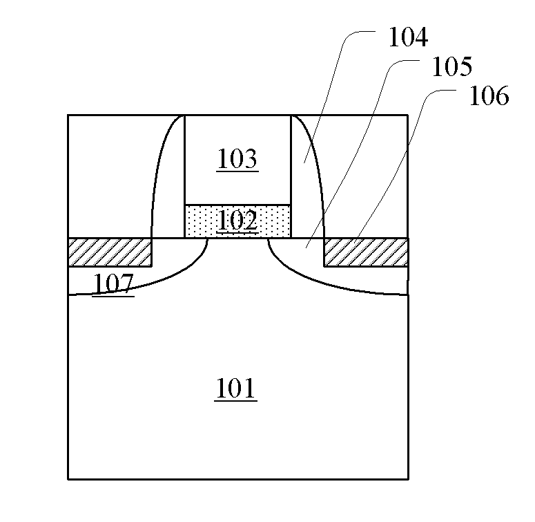
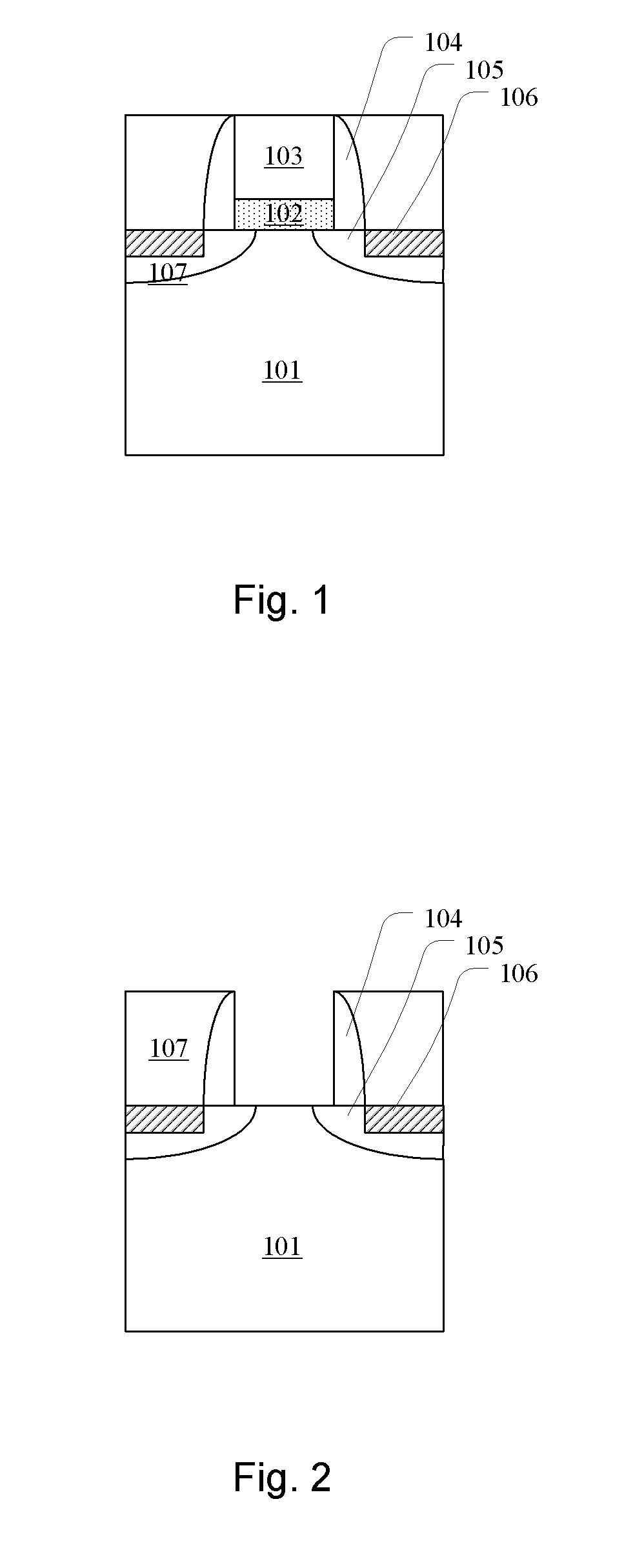
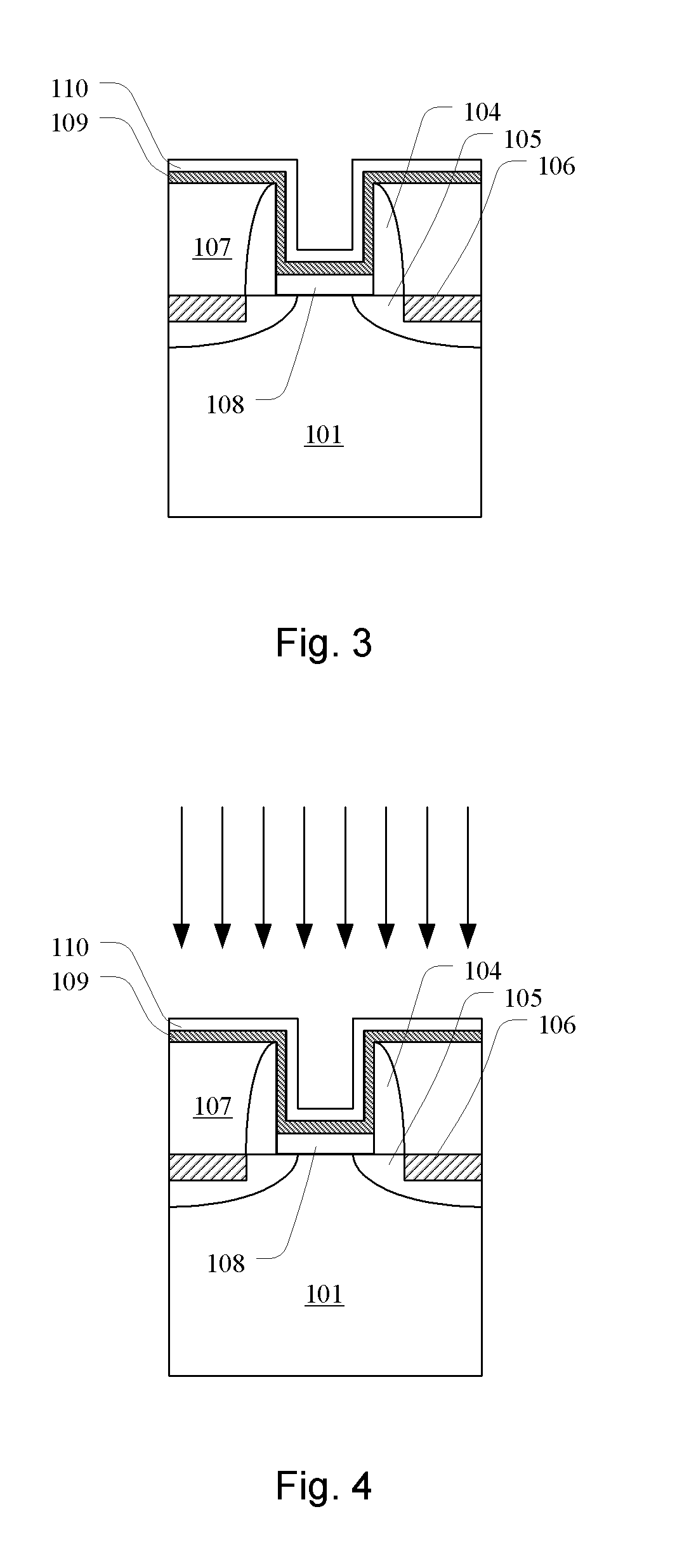
[0010]Next, the present disclosure will be described in detail with reference to the drawings. In the following description, similar parts will be indicated by identical or similar reference signs whether they are illustrated in different embodiments or not. Throughout the drawings, respective parts are not drawn to scale for purpose of clarity.

[0011]Specific details of the present disclosure, such as structures, materials, sizes, processes and technologies of devices, are described below to facilitate understanding of the present disclosure. However, those skilled in the art will understand that the present disclosure can be implemented without these specific details. Unless otherwise specified, respective parts of a semiconductor device may comprise materials known to those skilled in the art or future materials having similar characteristics.

[0012]In the present disclosure, the term “semiconductor structure” refers to a semiconductor substrate and all layers or regions that have ...


PUM


Abstract

The present disclosure discloses a method for manufacturing an N-type MOSFET, comprising: forming a part of the MOSFET on a semiconductor substrate, the part of the MOSFET comprising source/drain regions in the semiconductor substrate, a replacement gate stack between the source/drain regions above the semiconductor substrate, and a gate spacer surrounding the replacement gate stack; removing the replacement gate stack of the MOSFET to form a gate opening exposing a surface of the semiconductor substrate; forming an interface oxide layer on the exposed surface of the semiconductor; forming a high-K gate dielectric layer on the interface oxide layer in the gate opening; forming a first metal gate layer on the high-K gate dielectric layer; implanting dopant ions into the first metal gate layer; and performing annealing to cause the dopant ions to diffuse and accumulate at an upper interface between the high-K gate dielectric layer and the first metal gate layer and a lower interface between the high-K gate dielectric layer and the interface oxide layer, and also to generate electric dipoles by interfacial reaction at the lower interface between the high-K gate dielectric layer and the interface oxide layer.

Description

CROSS-REFERENCE TO RELATED APPLICATION(S) [0001]This application claims priority to Chinese Application No. 201210506435.4, filed on Nov. 30, 2012, entitled “METHOD FOR MANUFACTURING N-TYPE MOSFET,” which is incorporated herein by reference it is entirety.TECHNICAL FIELD [0002]The present disclosure relates to a technical field of semiconductor, and in particular, to a method for manufacturing an N-type MOSFET comprising a metal gate and a high-K gate dielectric layer.BACKGROUND [0003]With development of semiconductor technology, feature size of Metal Oxide Semiconductor Field Effect Transistors (MOSFETs) decreases continuously. The reduced size of the MOSFET may cause a current leakage problem. Physical thickness of a gate dielectric layer can be increased without changing Equivalent Oxide Thickness (EOT) by use of a high-K gate dielectric layer, so as to reduce tunneling leakage current. However, a conventional poly-silicon gate is incompatible with the high-K gate dielectric laye...

Claims


Application Information

Patent Timeline
IPC IPC(8): H01L29/66
CPCH01L21/28176H01L21/28088H01L29/4966H01L29/513H01L29/517H01L29/518H01L29/66545
Inventor XU, QIUXIAZHU, HUILONGZHOU, HUAJIEXU, GAOBO
Owner INST OF MICROELECTRONICS CHINESE ACAD OF SCI
Why Eureka
Try Eureka