Pec etching of (20-2-1) semipolar gallium nitride for external efficiency enhancement in light emitting diode applications

a technology of light-emitting diodes and semi-polar gans, applied in semiconductor/solid-state device manufacturing, semiconductor devices, electrical apparatus, etc., can solve the problems of difficult to achieve high-quality crystal growth of 11-20 non-polar devices, and low efficiency of 2021 semi-polar gans. achieve the effect of improving the efficiency of semi-polar gan based led performan

Inactive Publication Date: 2014-06-19
RGT UNIV OF CALIFORNIA
View PDF3 Cites 4 Cited by
  • Summary
  • Abstract
  • Description
  • Claims
  • Application Information

AI Technical Summary

Benefits of technology

[0016]To overcome the limitations in the prior art described above, and to overcome other limitations that will become apparent upon reading and understanding the present specification, the present invention discloses a method of photoelectrochemical (PEC) etching of {20-2-1} semipolar GaN for surface roughening of light emitting devices to improve light extraction and enhance external efficiency. Using the present invention results in improved semipolar GaN based LED performance. The surface morphology of {20-2-1} semipolar GaN showed significant roughening with a much higher root mean square (RMS) roughness, scanned by atomic force microscopy (AFM), as compared to other semipolar planes under the same etching conditions. This roughened surface morphology resulting from PEC etching can be an economical and rapid technique for enhancing the extraction efficiency of semipolar GaN LEDs and LDs.

Problems solved by technology

LEDs and LDs grown on polar and semipolar planes suffer from polarization related electric fields in the quantum wells that degrade device performance.
While {10-10} and {11-20} nonpolar devices are free from polarization related effects, incorporation of high Indium concentrations in {10-10} nonpolar devices and high quality crystal growth of {11-20} nonpolar devices have been shown to be difficult to achieve.

Method used


Image

  • Pec etching of (20-2-1) semipolar gallium nitride for external efficiency enhancement in light emitting diode applications
  • Pec etching of (20-2-1) semipolar gallium nitride for external efficiency enhancement in light emitting diode applications
  • Pec etching of (20-2-1) semipolar gallium nitride for external efficiency enhancement in light emitting diode applications

Examples


Embodiment Construction

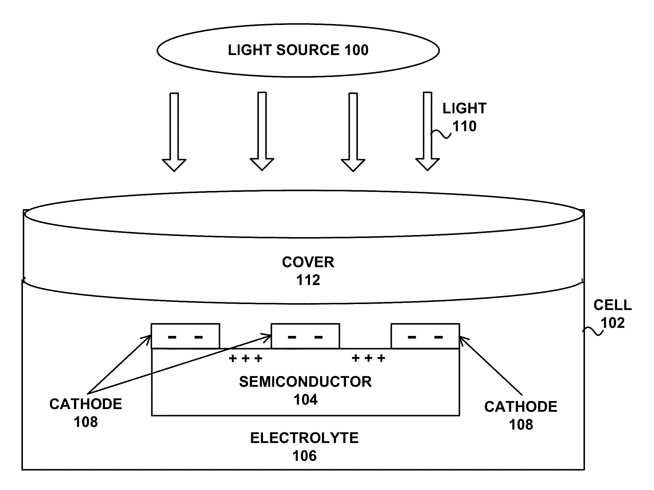
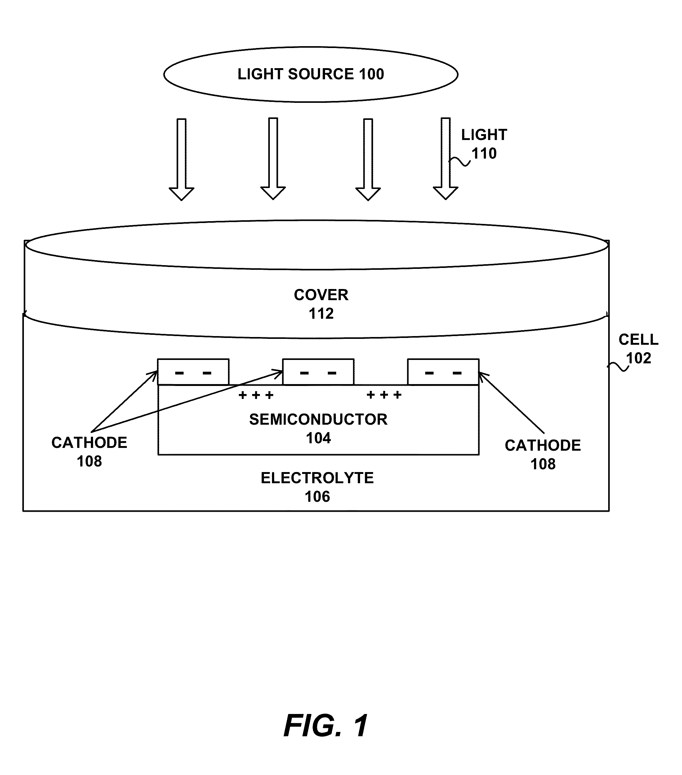
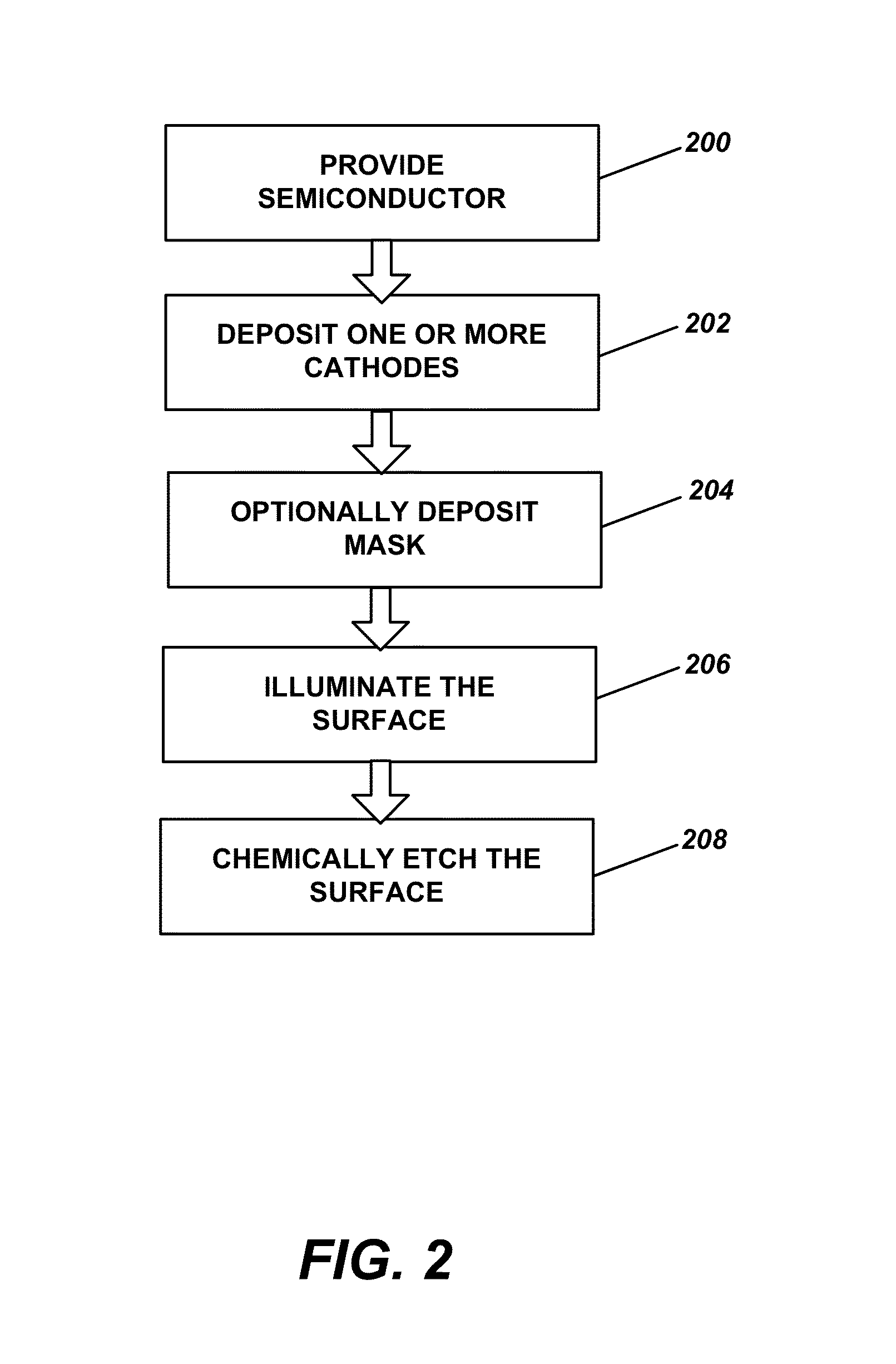
[0023]In the following description of the preferred embodiment, reference is made to the accompanying drawings which form a part hereof, and in which is shown by way of illustration a specific embodiment in which the invention may be practiced. It is to be understood that other embodiments may be utilized and structural changes may be made without departing from the scope of the present invention.

Etching Apparatus

[0024]FIG. 1 is a schematic that illustrates the apparatus used in the PEC etching of the present invention, wherein the PEC etching is a photo-assisted wet etch process that can be used to etch III-nitride semiconductors including GaN and its alloys. The apparatus is comprised of a light source 100 and an electrochemical cell 102, where a semiconductor 104 immersed in an electrolyte 106 acts as an anode and the semiconductor 104 has metal in contact therewith or patterned directly thereon that act as cathodes 108. Light 110 from the light source 100 generates electron-hole...


PUM

PropertyMeasurementUnit
RMS) roughnessaaaaaaaaaa
RMS roughnessaaaaaaaaaa

Abstract

A method of performing a photoelectrochemical (PEC) etch on an exposed surface of a semipolar {20-2-1} III-nitride semiconductor, for improving light extraction from and for enhancing external efficiency of one or more active layers formed on or above the semipolar {20-2-1} III-nitride semiconductor.

Description

CROSS REFERENCE TO RELATED APPLICATIONS[0001]This application claims the benefit under 35 U.S.C Section 119(e) of the following co-pending and commonly-assigned patent application:[0002]U.S. Provisional Patent Application Ser. No. 61 / 695,124, filed on Aug. 30, 2012, by Chung-Ta Hsu, Chia-Yen Huang, Yuji Zhao, Shih-Chieh Haung, Daniel F. Feezell, Steven P. DenBaars, Shuji Nakamura, and James S. Speck, and entitled “PEC ETCHING OF {20-2-1} SEMIPOLAR GALLIUM NITRIDE FOR SEMIPOLAR FOR EXTERNAL EFFICIENCY ENHANCEMENT IN LIGHT EMITTING DIODE APPLICATIONS,” attorney's docket number 30794.466-US-P1 (2013-034-1);[0003]which application is incorporated by reference herein.[0004]This application is related to the following co-pending and commonly-assigned patent applications:[0005]U.S. Utility patent application Ser. No. 13 / 283,259, filed on Oct. 27, 2011, by Yuji Zhao, Junichi Sonoda, Chih-Chien Pan, Shinichi Tanaka, Steven P. DenBaars, and Shuji Nakamura, entitled “HIGH POWER, HIGH EFFICIENC...

Claims


Application Information

Patent Timeline
Patent Type & Authority Applications(United States)
IPC IPC(8): H01L33/00H01L33/32
CPCH01L33/32H01L33/0075H01L21/02389H01L21/0243H01L21/02433H01L21/0254H01L21/02658H01L33/007H01L33/16
Inventor HSU, CHUNG-TAHUANG, CHIA-YENZHAO, YUJIHAUNG, SHIH-CHIEHFEEZELL, DANIEL F.DENBAARS, STEVEN P.NAKAMURA, SHUJISPECK, JAMES S.
Owner RGT UNIV OF CALIFORNIA
Why Eureka
Try Eureka