Spin hall effect magnetic apparatus, method and applications

Active Publication Date: 2014-06-19
CORNELL UNIVERSITY
View PDF4 Cites 126 Cited by
  • Summary
  • Abstract
  • Description
  • Claims
  • Application Information

AI Technical Summary

Benefits of technology

[0016]A particular ST-MRAM structure in accordance with the embodiments includes a spin Hall effect base layer located over a substrate. The particular structure also includes a magnetic free layer located over the substrate and contacting the spin Hall effect base layer. Within the structure, a non-magnetic conductor material that comprises the spin Hall effect base layer has: (1) a spin Hall angle greater than about 0.05; and (2) a thickness no greater than about 5 times a spin diffusion length in the non-magnetic conductor material.
[0017]Another particular ST-MRAM structure in accordance with the embodiments includes a spin Hall effect base layer located over a substrate and including two laterally separated terminals This other particular structure also includes a magnetoresistive stack located contacting the spin Hall effect base layer and comprising: (1) a magnetic free layer located contacting the spin Hall effect base layer; (2) a non-magnetic spacer layer located over the magnetic free layer; and (3) a pinned layer located over the non-magnetic spacer layer. This other particular structure also includes a third terminal electrically connected to the pinned layer. Within this other particular structure, a non-magnetic conductor material that comprises the spin Hall effect base layer has: (1) a spin Hall angle greater than about 0.05; and (2) a thickness no greater than about 5 times a spin diffusion length in the non-magnetic conductor material.
[0018]A particular method for fabricating the ST-MRAM str

Problems solved by technology

Compared to conventional current induced switching in magnetic tunnel junctions, the SHE device geometry also provides a separation of the cu

Method used


Image

  • Spin hall effect magnetic apparatus, method and applications
  • Spin hall effect magnetic apparatus, method and applications
  • Spin hall effect magnetic apparatus, method and applications

Examples


Example

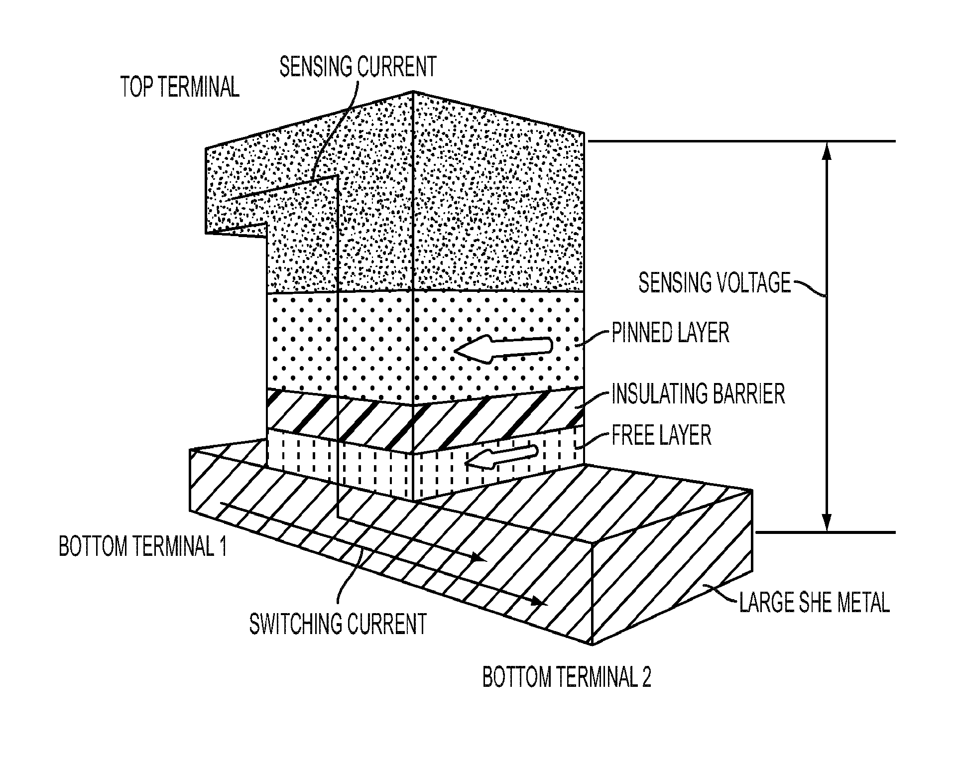
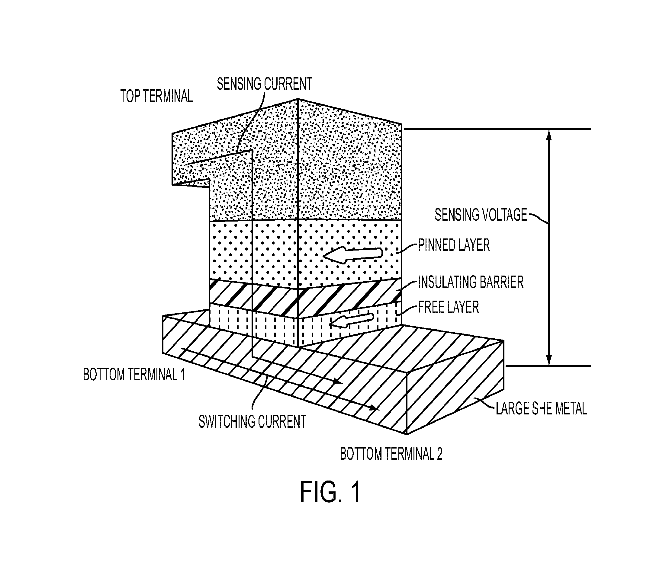
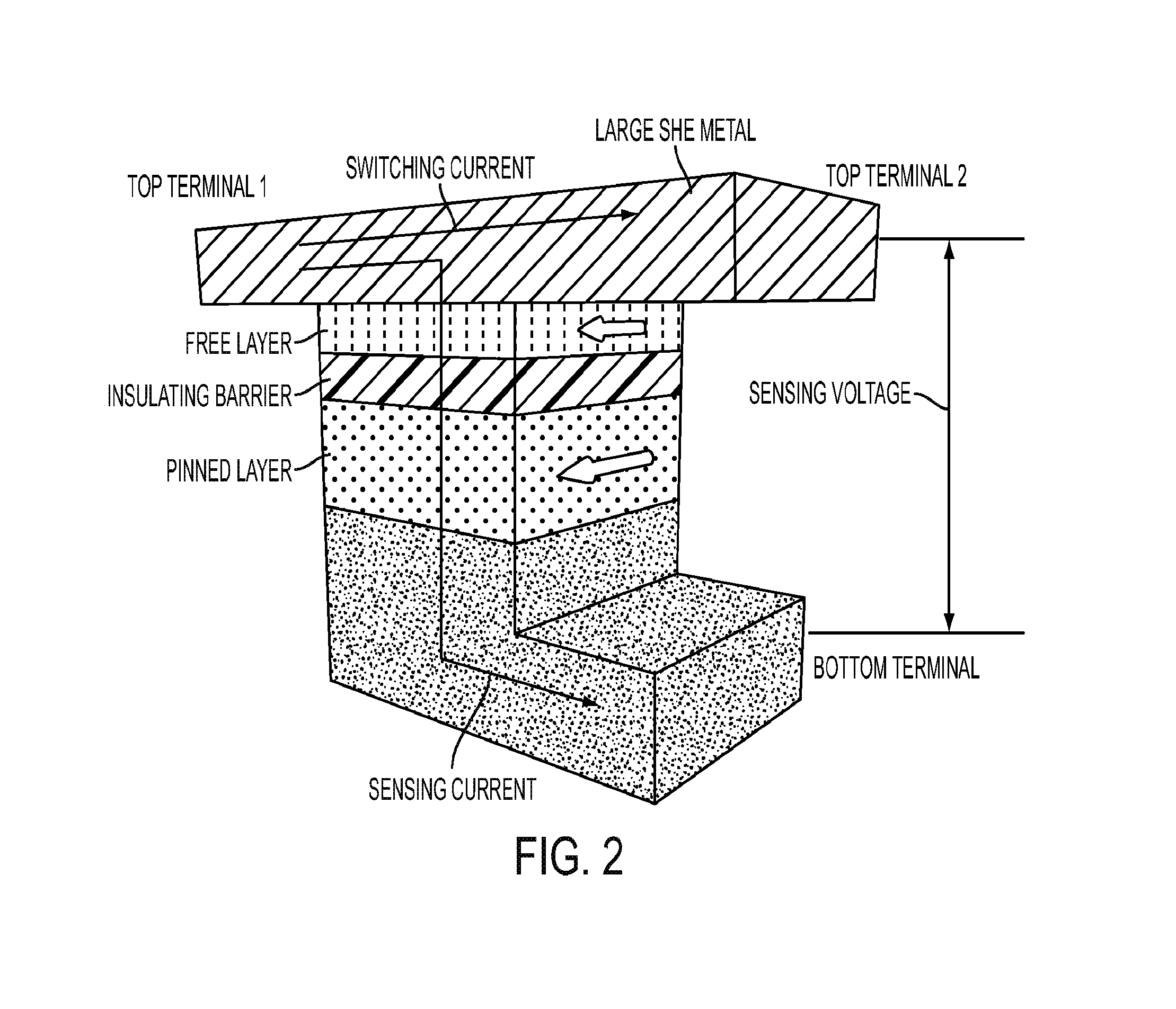
[0042]Embodiments include a spin torque magnetic random access memory (ST-MRAM) structure, a method for fabricating the ST-MRAM structure and a method for operating a ST-MRAM device that results from the ST-MRAM structure. The ST-MRAM structure and device in accordance with the embodiments use a spin Hall effect base layer located and formed contacting a free layer within the ST-MRAM structure and device so that a lateral current through the SHE base layer may be used to switch a magnetic orientation of a free layer with respect to a pinned layer while measuring or applying a sense voltage and a sense current perpendicularly through a magnetoresistive element stack that comprises the pinned layer, a non-magnetic spacer layer and the free layer that contacts the spin Hall effect base layer.

[0043]The embodiments contemplate that specific materials may be used for the spin Hall effect base layer, such as but not limited to Ta and W, with the high-resistivity beta forms of Ta and W bein...


PUM


Abstract

An ST-MRAM structure, a method for fabricating the ST-MRAM structure and a method for operating an ST-MRAM device that results from the ST-MRAM structure each utilize a spin Hall effect base layer that contacts a magnetic free layer and effects a magnetic moment switching within the magnetic free layer as a result of a lateral switching current within the spin Hall effect base layer. This resulting ST-MRAM device uses an independent sense current and sense voltage through a magnetoresistive stack that includes a pinned layer, a non-magnetic spacer layer and the magnetic free layer which contacts the spin Hall effect base layer. Desirable non-magnetic conductor materials for the spin Hall effect base layer include certain types of tantalum materials and tungsten materials that have a spin diffusion length no greater than about five times the thickness of the spin Hall effect base layer and a spin Hall angle at least about 0.05.

Description

CROSS-REFERENCE TO RELATED APPLICATION[0001]This application is related to, and derives priority from: (1) U.S. Provisional Patent Application Ser. No. 61 / 524,998, filed Aug. 18, 2011; (2) U.S. Provisional Patent Application Ser. No. 61 / 534,517, filed Sep. 14, 2011; (3) U.S. Provisional Patent Application Ser. No. 61 / 545,705, filed Oct. 11, 2011; and (4) U.S. Provisional Patent Application Ser. No. 61 / 619,679, filed Apr. 3, 2012, each titled Spin Hall Effect Apparatus, Method and Applications, the content of each of which provisional patent application is incorporated herein fully by reference.STATEMENT OF GOVERNMENT INTEREST[0002]The research that lead to the embodiments as disclosed herein and the invention as claimed herein was funded by the United States Army Research Office under award W911NF-08-2-0032, the United States Defense Advanced Research Project Agency, under award HR0011-11-C-0074, and the United States Office of Naval Research under award N00014-10-1-0024. The United...

Claims


Application Information

Patent Timeline
IPC IPC(8): H01L43/04G11C16/30H01L43/14
CPCH01L43/04H01L43/14G11C16/30G11C11/18H01F10/3254H01F10/3286G11C11/161G11C11/1675H10N50/80H10N50/01H10N50/10G11C11/1673H10N52/01H10N52/80
Inventor BUHRMAN, ROBERT A.LIU, LUQIAORALPH, DANIEL C.PAI, CHI-FENG
Owner CORNELL UNIVERSITY
Why Eureka
Try Eureka