System and method for detecting infrared radiation
- Summary
- Abstract
- Description
- Claims
- Application Information
AI Technical Summary
Benefits of technology
Problems solved by technology
Method used
Image

Examples
first embodiment
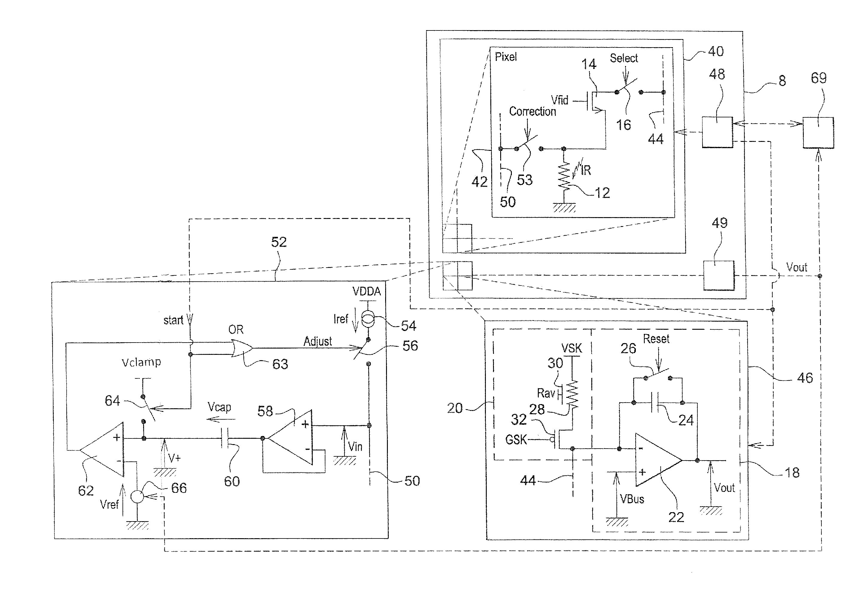
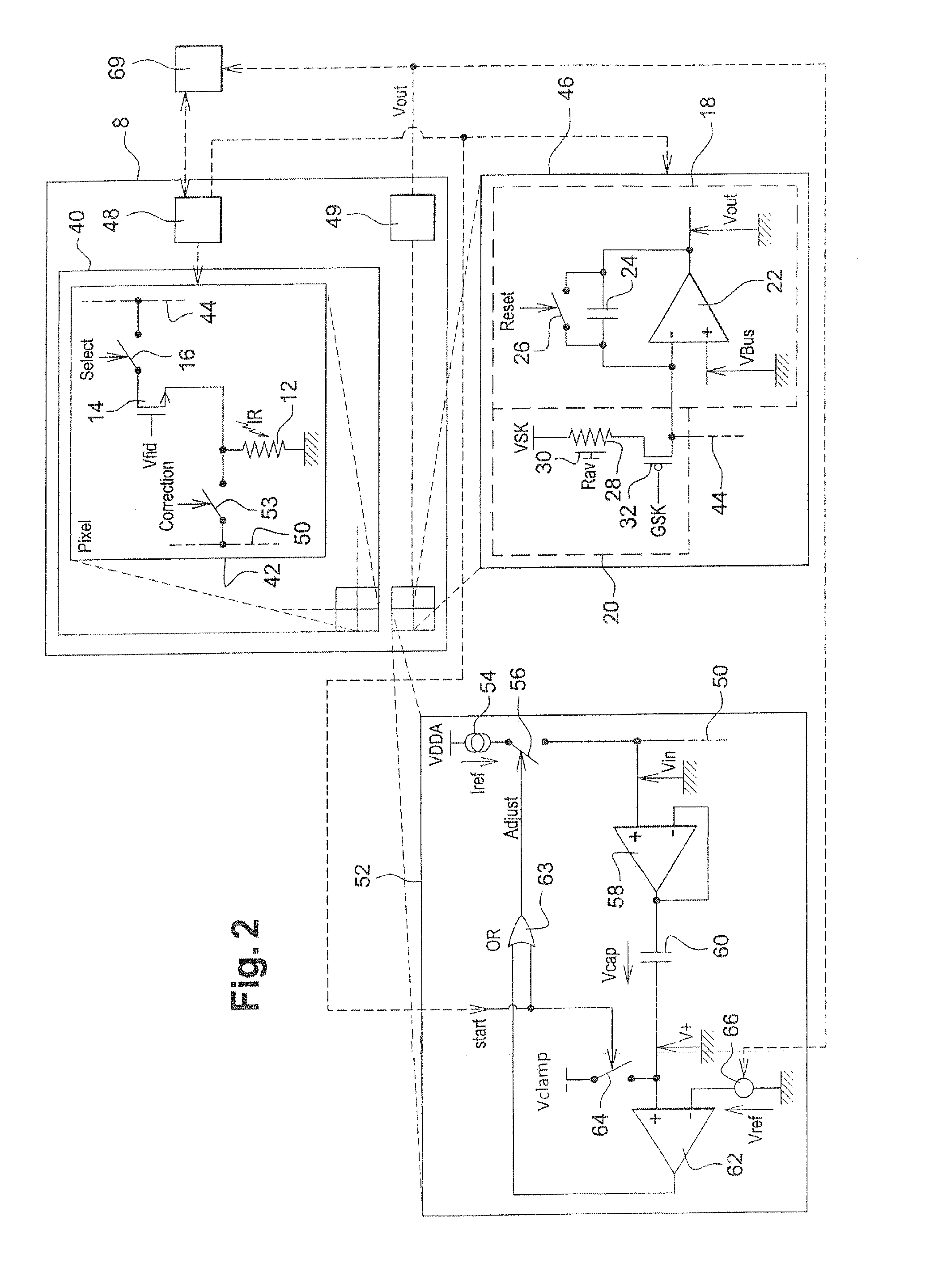
[0086] control circuitry 52 comprises:[0087]a current source 54 that outputs a constant predetermined current Iref and has one of its terminals connected to a constant voltage source VDDA, the current Iref being identical for all the control circuitries 52;[0088]a first controllable switch 56 connected between the other terminal of current source 54 and column correction bus 50;[0089]an operational amplifier 58 whose non-inverting input (+) is connected to column correction bus 50. The inverting input (−) of amplifier 58 is connected to the latter's output so that amplifier 58 thus operates as a voltage follower;[0090]a capacitor 60 that has one of its terminals connected to the output of amplifier 58;[0091]a comparator 62, the positive input (+) of which is connected to the other terminal of capacitor 60 and the output of which controls opening and closing of switch 56 through an OR logic gate 63;[0092]a second switch 64 that can be controlled by means of a “Start” signal by timer ...
third embodiment
[0169]Thus, according to the invention, a table Δt is calculated and stored in the memory of the management unit 69, which contains the individual temperature-rise durations Δt(i,j) that are to be applied in order to produce the individual ΔR0(i,j) quantities. The correction phase for a row of array 40 of pixels 12 thus involves loading the corresponding Δt(i,j) duration values in interval timers 142, closing switches 56 (switches 16 remain open and switch 53 is closed) and then opening each of them after an individually customized duration. The resistance of each of bolometers 12 of a row is thus corrected by their corresponding quantity ΔR0(i,j).
fourth embodiment
[0170] it may be advantageous to bias the bolometers under a spatially uniform and constant voltage Vpol between its terminals during individually pre-calculated time intervals Δt(i,j), the currents in the bolometers being free to change based on the resistance variation induced by the Joule effect. This embodiment differs from the embodiment in FIG. 2 by virtue of the control circuits for the resistances 52 of bolometers 12.
[0171]For doing so, as shown on FIG. 9B, any constant (that is to say spatially uniform along the row being corrected and sequentially identical from row to row) voltage Vpol 58 able to heat up the more resistive bolometer so as to produce the highest resistance variation ΔR0 MAX during a line period might be used. This insures that all bolometers of the ith line would be properly tweaked in resistance within the time the (i−1)th line is being read.
[0172]Advantageously, the reduced voltage that was selected for biasing the bolometers during the calibration phase...
PUM
 Abstract
Description
Claims
Application Information