Copper electroplating solution and copper electroplating apparatus

a technology of electroplating solution and copper, which is applied in the direction of electrolysis process, electrolysis components, semiconductor devices, etc., can solve the problems of uneven solder bump, metal is excessively plated at some points and insufficiently plated at other points, and the flatness of the solder bump is deteriorated, so as to increase the overall electroplating process of copper. , the effect of increasing the process efficiency of the electroplating process

Active Publication Date: 2014-07-17
SAMSUNG ELECTRONICS CO LTD
View PDF5 Cites 8 Cited by
  • Summary
  • Abstract
  • Description
  • Claims
  • Application Information

AI Technical Summary

Benefits of technology

[0041]According to example embodiments of the present inventive concepts, a copolymer from which nitrogen positive ions may be dissolved may be mixed with the aqueous electrolyte solution as the leveler of the electroplating solution. Thus, abnormal precipitation of copper may be sufficiently prevented or inhibited at a relatively high current area at which the charge density may be locally higher over an average charge density. Accordingly, the process efficiency of the electroplating process for forming the copper bump may be sufficiently increased without deterioration of the surface flatness of the copper bump, thereby increasing an overall electroplating process of the copper.

Problems solved by technology

However, the uniformity of the solder bump and the uniform metal plating usually conflicts with the electroplating speed, and thus the uniform metal plating and the plating speed has trade-off relations.
In contrast, the current of relatively high intensity in the electroplating process usually causes locally abnormal growth of the electroplated metal and the non-uniform metal plating, which results in the non-uniformity of the solder bump.
When the electrical current is applied to the IC chip at a relatively high intensity, the metal plating is likely to be performed locally under an unsteady state and thus the metal is excessively plated at some points and is insufficiently plated at other points.
Therefore, the surface flatness of the solder bump is deteriorated and thus the surface area with which external bodies make contact is insufficient for the semiconductor package.
However, an electroplating solution of which the metal can be uniformly plated at a relatively high speed has not yet been suggested, especially for the electroplating metal of copper (Cu).

Method used


Image

  • Copper electroplating solution and copper electroplating apparatus
  • Copper electroplating solution and copper electroplating apparatus
  • Copper electroplating solution and copper electroplating apparatus

Examples


Embodiment Construction

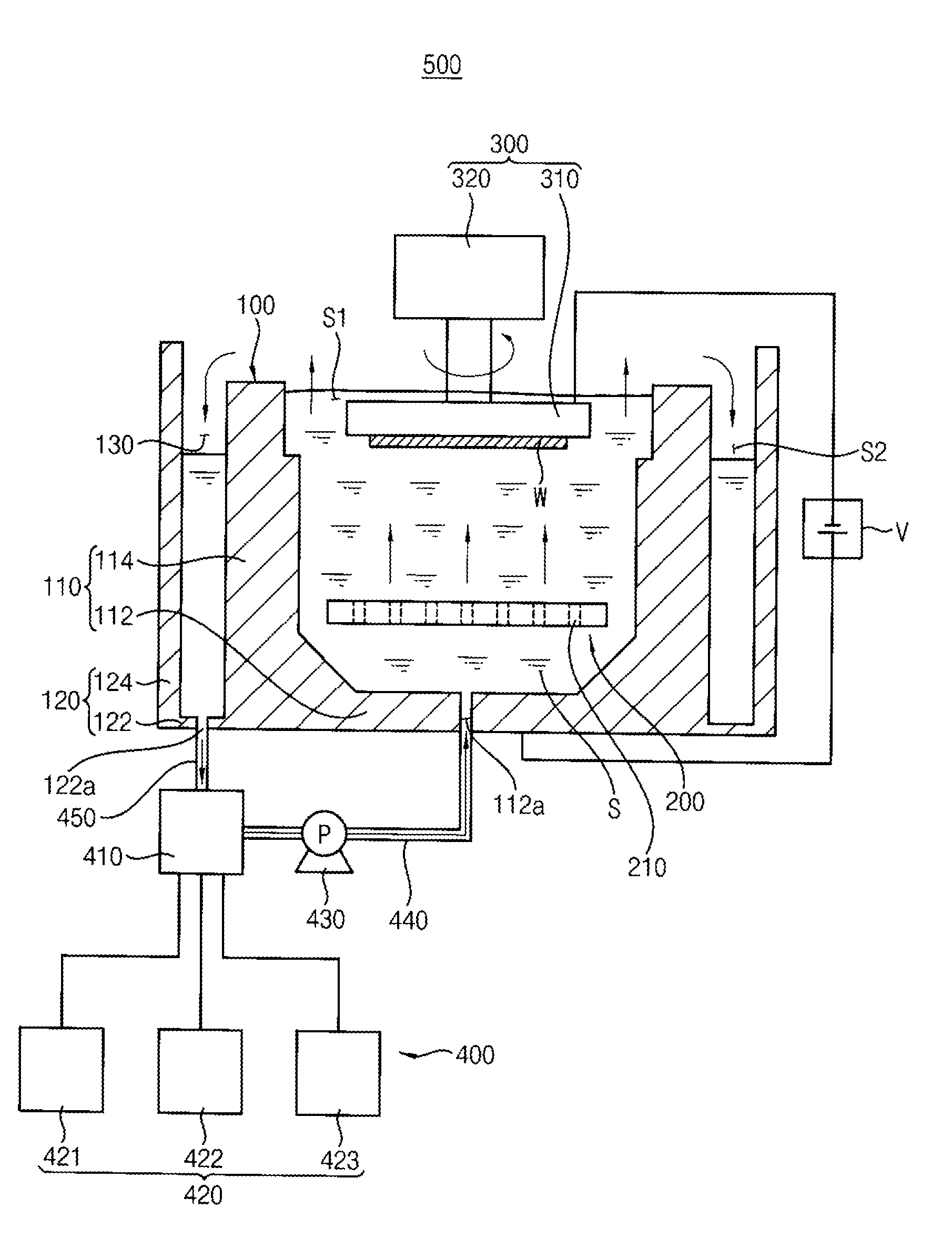
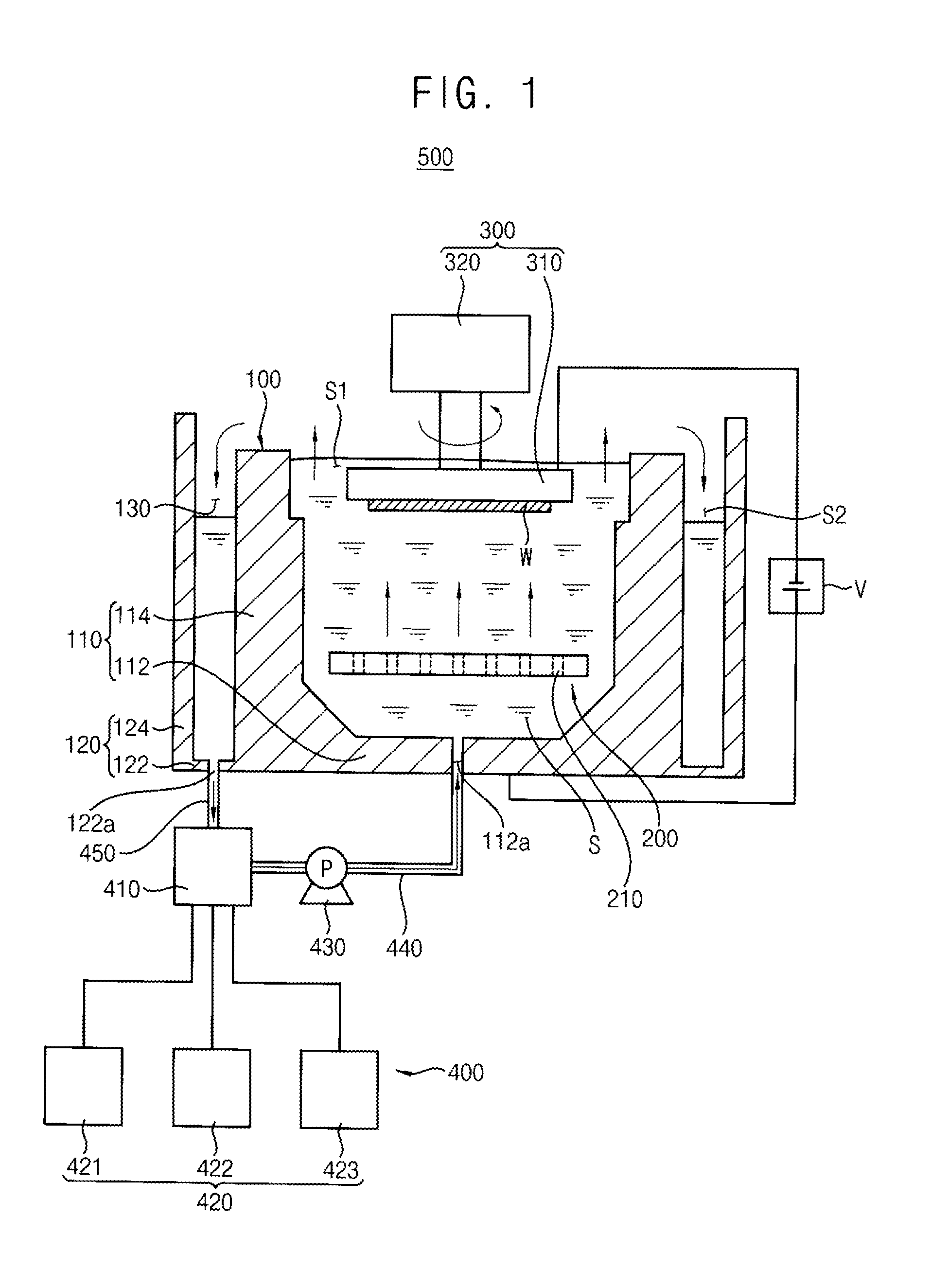
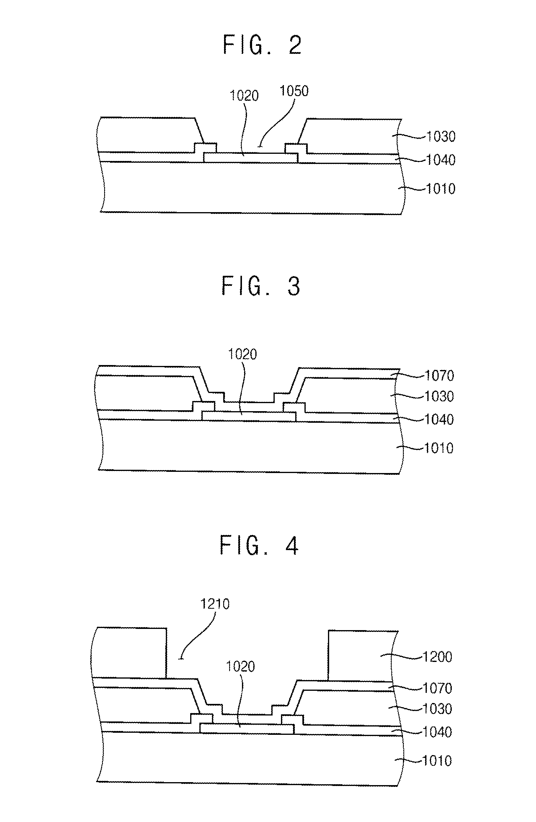
[0048]Various example embodiments will be described more fully hereinafter with reference to the accompanying drawings, in which some example embodiments are shown. The present inventive concepts may, however, be embodied in many different forms and should not be construed as limited to the example embodiments set forth herein. Rather, these example embodiments are provided so that this disclosure will be thorough and complete, and will fully convey the scope of the present inventive concepts to those skilled in the art. In the drawings, the sizes and relative sizes of layers and regions may be exaggerated for clarity.

[0049]It will be understood that when an element or layer is referred to as being “on,”“connected to” or “coupled to” another element or layer, it can be directly on, connected or coupled to the other element or layer or intervening elements or layers may be present. In contrast, when an element is referred to as being “directly on,”“directly connected to” or “directly...


PUM

PropertyMeasurementUnit
concentrationaaaaaaaaaa

Abstract

An electroplating solution includes an aqueous electrolyte solution including water soluble copper salts, sulfide ions and chloride ions, an accelerator including an organic material having sulfur (S), the accelerator accelerating copper (Cu) reduction, a suppressor including a polyether compound, the suppressor selectively suppressing the copper reduction, and a leveler including a water soluble polymer having nitrogen that is dissolved into positive ions in the aqueous electrolyte solution.

Description

CROSS-REFERENCE TO RELATED APPLICATIONS[0001]This application claims the benefit of Korean Patent Application No. 10-2013-0004909 filed on Jan. 16, 2013 in the Korean Intellectual Property Office, the disclosure of which is incorporated herein in its entirety by reference.BACKGROUND[0002]1. Field[0003]Example embodiments relate to a copper electroplating solution, a copper electroplating apparatus and a method of forming a copper bump using the electroplating apparatus. More particularly, example embodiments relate to a copper electroplating solution and a copper electroplating apparatus for forming a bump on a flip chip and a method of forming the bump using the copper electroplating apparatus.[0004]2. Description of the Related Art[0005]Conventional semiconductor packages and board structure for a semiconductor package, for example, a printed circuit board (PCB), usually have contact terminals for electrically communicating with external bodies. For example, solder bumps and solde...

Claims


Application Information

Patent Timeline
Patent Type & Authority Applications(United States)
IPC IPC(8): C25D3/38
CPCC25D3/38C25D5/04C25D5/08C25D17/001C25D17/06C25D21/14C25D5/022C25D5/50C25D7/123C25D21/10
Inventor PARK, MYUNG-BEOMKANG, YUN-DEOKKIM, KI-HYEONCHO, YOUN-JOUNGCHOI, JUNG-SIK
Owner SAMSUNG ELECTRONICS CO LTD
Why Eureka
Try Eureka