Defect observation method and device therefor

a technology of defect observation and detection method, applied in the direction of television system, semiconductor/solid-state device testing/measurement, instruments, etc., can solve the problems of difficult to secure accuracy, inability to detect minute heights by three-dimensional analysis, and inability to carry out high-accurate height measuremen

Inactive Publication Date: 2014-07-24
HITACHI HIGH-TECH CORP
View PDF1 Cites 25 Cited by
  • Summary
  • Abstract
  • Description
  • Claims
  • Application Information

AI Technical Summary

Benefits of technology

[0013]As three-dimensional shape analysis methods using an SEM, there are methods of deriving a three-dimensional shape from vectors of reflected electrons and deriving a three-dimensional shape from the shade of an obtained electron image. However, highly-accurate height measurement is not carried out in the current situation because the deriving is technically difficult and it is difficult to secure the accuracy. Further, minute heights cannot be detected by the three-dimensional analysis using an SEM because detectors are provided on the upper side.

Problems solved by technology

However, highly-accurate height measurement is not carried out in the current situation because the deriving is technically difficult and it is difficult to secure the accuracy.
Further, minute heights cannot be detected by the three-dimensional analysis using an SEM because detectors are provided on the upper side.
However, it is necessary to irradiate light on a sample using highly-accelerated voltage in order to specify the material, and thus the sample is extremely damaged.
In addition, it is difficult to specify the material of minute defects because the resolution is poor.
Further, defects that cannot be detected by an SEM include foreign substances in or under a membrane, crystal defects, and the like.
As a cause of the impossibility, there is a difference in the penetration depth between the illumination of an optical inspection device and the illumination of a review device.
For the defects that cannot be detected by an SEM, it is difficult to determine whether information of the optical inspection device is false or the defects actually exist.
Further, it is impossible to derive the shapes and depths of the defects.

Method used


Image

  • Defect observation method and device therefor
  • Defect observation method and device therefor
  • Defect observation method and device therefor

Examples


Embodiment Construction

[0037]Hereinafter, an embodiment of the present invention will be described in detail by appropriately using the drawings.

[0038]In general, in the case where defects generated on a substrate are observed in a semiconductor manufacturing process, the observation is performed in accordance with the following defect observation procedure. First, the entire surface of a sample is scanned by an inspection device to detect defects existing on the sample, and the coordinates where the defects exist are obtained. Next, some or all of the defects detected by the inspection device are observed in detail by a review device on the basis of the defect coordinates detected by the inspection device, so that the defects are classified and the cause of generation is analyzed.

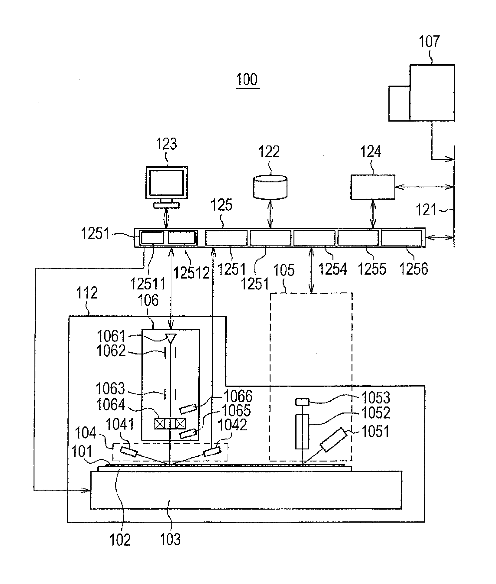
[0039]An example of a configuration of a review device 100 in the present invention is shown in FIG. 1. The review device 100 of the embodiment includes a sample holder 102 on which a sample 101 to be inspected is mounted, a sta...


PUM

PropertyMeasurementUnit
penetration depthaaaaaaaaaa
defect observation methodaaaaaaaaaa
scanning electron microscopeaaaaaaaaaa

Abstract

This invention relates to a method for performing an analysis of defective material and the refractive index, and a three-dimensional analysis of very small pattern shapes including the steps of imaging by a scanning electron microscope to acquire an image of the position of a defect under observation using information of inspection results obtained by an optical inspection device, creating a model of the defect by using the acquired image of the defect under observation, calculating the values detected by the detector when reflected and scattered light emitted from a defect model is received by the detector when light is irradiated onto the defect model thus created, comparing the detection values thus calculated and the values detected by the detector, which has received light actually reflected and scattered from the sample, to obtain information relating to the height of the defect under observation, the material, or the refractive index.

Description

BACKGROUND[0001]The present invention relates to a defect observation method and a device therefor in which defects and the like existing on or near the surface of a sample detected by a defect inspection device are observed.[0002]For example, existence of foreign substances on a semiconductor substrate (wafer) and pattern defects such as short circuits or disconnections (hereinafter, these are collectively described as defects) causes failure such as insulation failure or short circuits of lines in a manufacturing process of a semiconductor device. With the advanced microfabrication of circuit patterns formed on a wafer, fine defects cause insulation failure of a capacitor and destruction of a gate oxide film or the like. These defects are mixed in various states due to various causes such as those generated from a movable part of a carrier device, generated from a human body, generated by reaction with process gas in a processing device, or mixed in chemicals or materials. Therefo...

Claims


Application Information

Patent Timeline
Patent Type & Authority Applications(United States)
IPC IPC(8): G01N21/95G02B26/00
CPCG02B26/008G01N21/9505G01B11/00G01B11/02G01B15/00H01L22/12G01N21/47G01N21/9501G01N2021/4711G01N2021/8822G01N2021/8867H01L2924/0002H01L2924/00
Inventor OTANI, YUKOHONDA, TOSHIFUMIURANO, YUTA
Owner HITACHI HIGH-TECH CORP
Why Eureka
Try Eureka