Stacked wafer DDR package

a technology of stacking wafers and memory dies, applied in semiconductor devices, semiconductor/solid-state device details, electrical apparatus, etc., can solve the problems of the size of the substrate used in the package, and the inability to provide the capability of newer and more powerful devices. , to achieve the effect of improving signal and power integrity in the top package and reducing the overall thickness of the top packag

Active Publication Date: 2014-07-31
APPLE INC
View PDF13 Cites 39 Cited by
  • Summary
  • Abstract
  • Description
  • Claims
  • Application Information

AI Technical Summary

Benefits of technology

[0009]The RDL may include routing between the first memory die and one or more first terminals coupled to the RDL on a periphery of the die. The RDL may also include electrically separate routing between the second memory die and one or more second terminals coupled to the RDL on a periphery of the die. The routing between the first memory die and the first terminals may be electrically isolated from the routing between the second memory die and the second terminals. The RDL reduces the overall thickness of the top package and improves signal and power integrity in the top package.

Problems solved by technology

One limitation in reducing the size of a package (e.g., either the top package (the memory package) or the bottom package (the SoC package) in the PoP package) is the size of the substrate used in the package.
The single memory die, however, may not provide sufficient capability for newer and more powerful devices.
Stacking the die vertically, however, creates problems with connecting both die to terminals on the package.
In addition, wire bonding may provide a high impedance path that reduces signal integrity and / or power integrity between the memory die and the terminals.
Providing TSVs, however, requires special memory die, adds several additional process steps, and is relatively expensive.

Method used


Image

  • Stacked wafer DDR package
  • Stacked wafer DDR package
  • Stacked wafer DDR package

Examples


Embodiment Construction

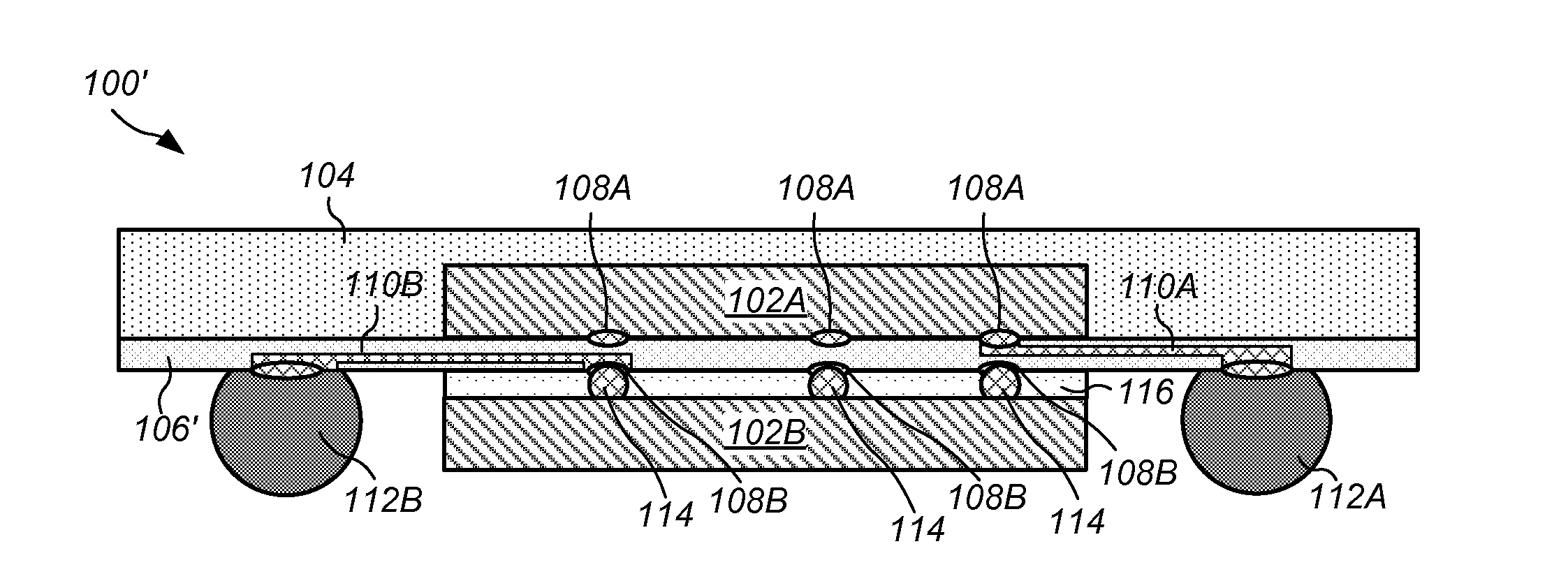
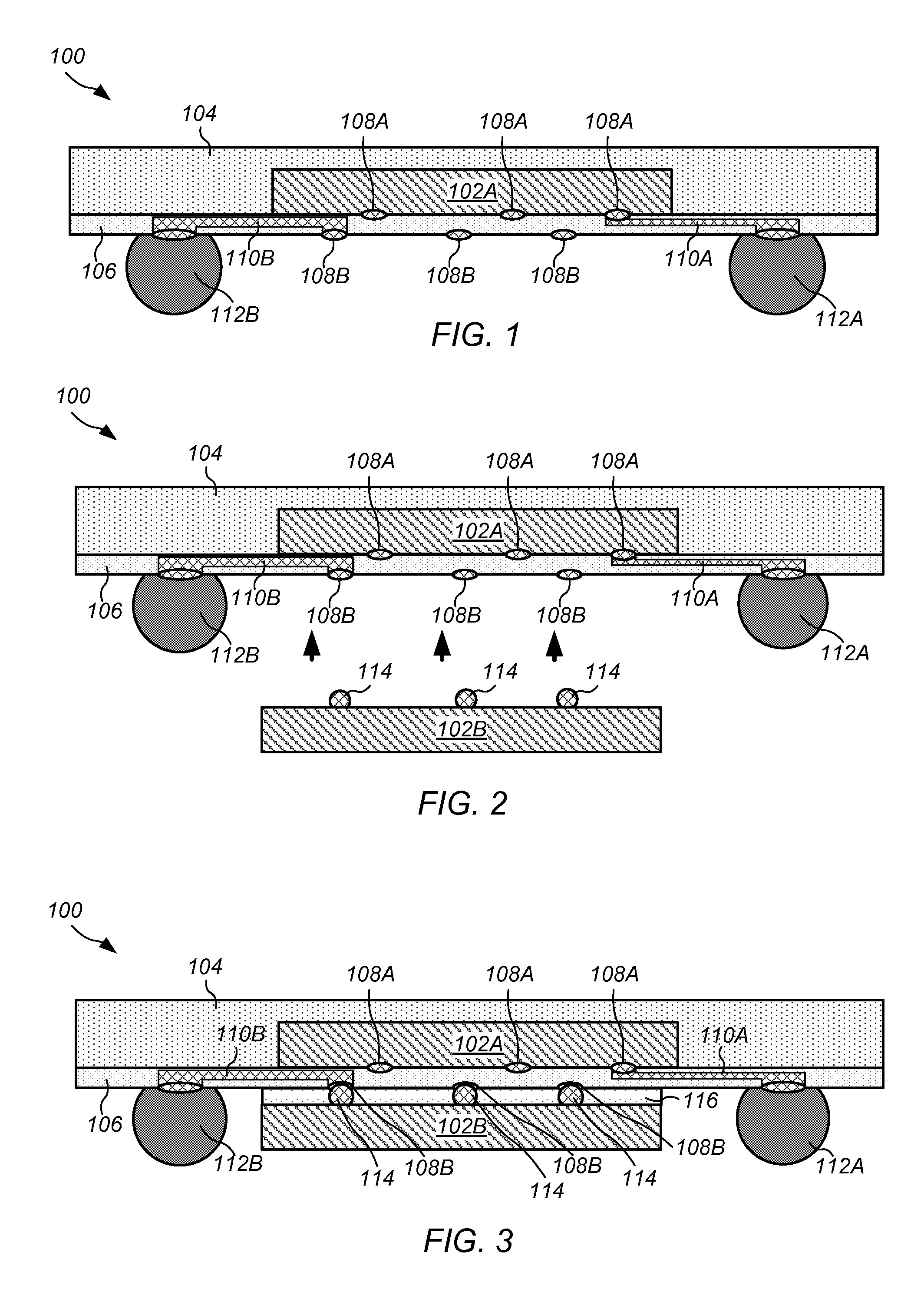
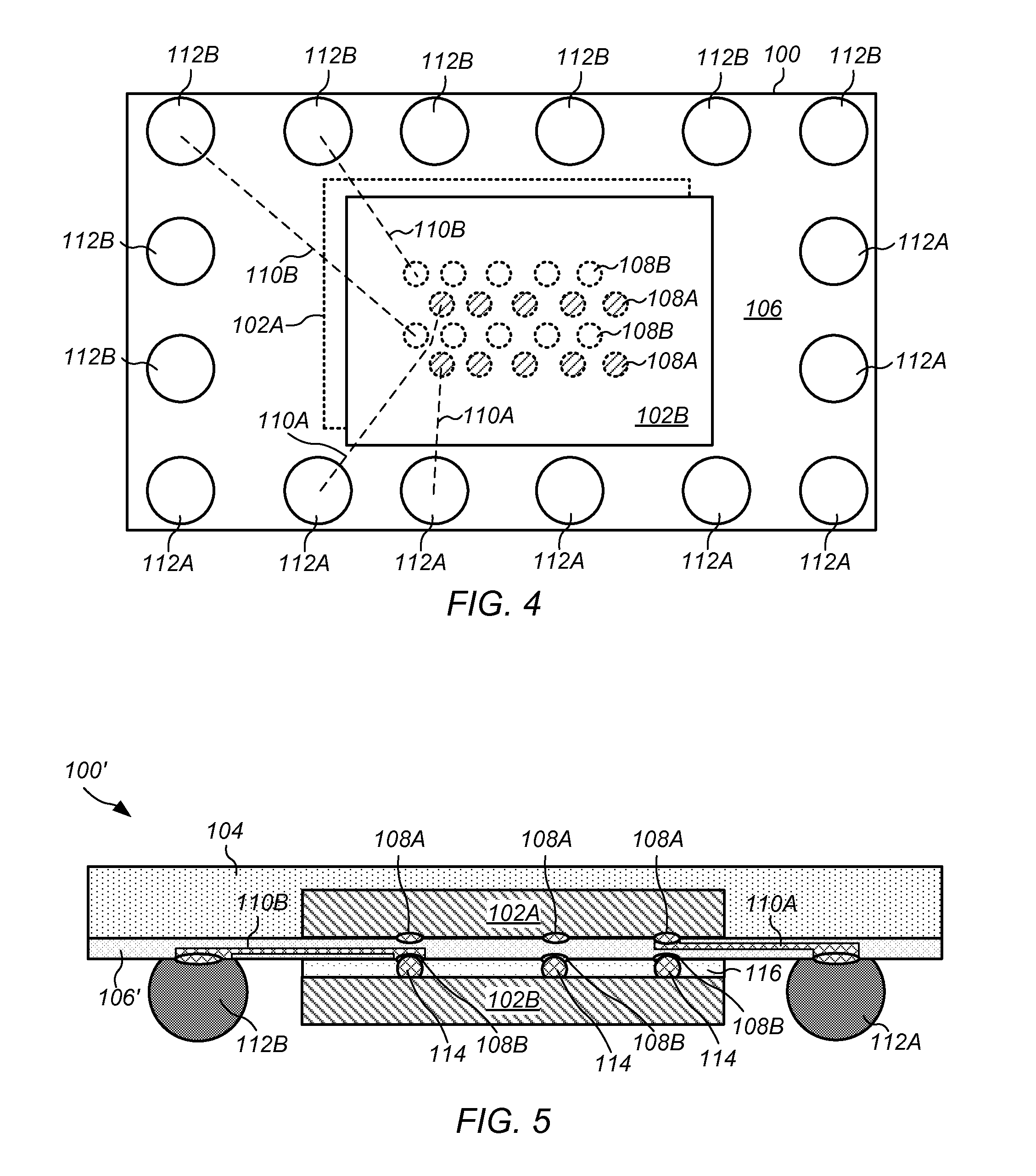
[0017]FIGS. 1-3 depict cross-sectional representations of steps of an embodiment of a process flow for forming a top package used in a PoP (“package-on-package”) package. FIG. 1 depicts a cross-sectional representation of an encapsulated memory die with a redistribution layer coupled to the memory die used in forming top package 100. Memory die 102A is at least partially encapsulated in encapsulant 104. In certain embodiments, a bottom surface of die 102A is exposed (uncovered) by encapsulant 104. Die 102A may be, for example, a semiconductor chip such as a wire-bond die or a flip chip die. In certain embodiments, die 102A is a DDR (double data rate) die (e.g., an 8 GB DDR die). Encapsulant 104 may be, for example, a polymer or a mold compound such as an overmold or exposed mold.

[0018]In certain embodiments, redistribution layer (RDL) 106 is coupled to die 102A. RDL 106 may be coupled to a bottom surface of die 102A. RDL 106 may also be coupled to encapsulant 104. RDL 106 may includ...


PUM


Abstract

A top package used in a PoP (package-on-package) package includes two memory die stacked with a redistribution layer (RDL) between the die. The first memory die is encapsulated in an encapsulant and coupled to a top surface of the RDL. A second memory die is coupled to a bottom surface of the RDL. The second memory die is coupled to the RDL with either a capillary underfill material or a non-conductive paste. The RDL includes routing between each of the memory die and one or more terminals coupled to the RDL on a periphery of the die.

Description

BACKGROUND[0001]1. Field of the Invention[0002]The present invention relates to semiconductor packaging and methods for packaging semiconductor devices. More particularly, the invention relates to a top package of a PoP (package-on-package) for memory die.[0003]2. Description of Related Art[0004]Package-on-package (“PoP”) technology has become increasingly popular as the demand for lower cost, higher performance, increased integrated circuit density, and increased package density continues in the semiconductor industry. As the push for smaller and smaller packages increases, the integration of die and package (e.g., “pre-stacking” or the integration of system on a chip (“SoC”) technology with memory technology) allows for thinner packages. Such pre-stacking has become a critical component for thin and fine pitch PoP packages.[0005]One limitation in reducing the size of a package (e.g., either the top package (the memory package) or the bottom package (the SoC package) in the PoP pac...

Claims


Application Information

Patent Timeline
Patent Type & Authority Applications(United States)
IPC IPC(8): H01L23/498H01L21/50
CPCH01L21/50H01L23/498H01L2225/06527H01L23/3128H01L23/49816H01L25/03H01L2224/16145H01L2225/06517H01L2225/06572H01L23/49827H01L24/13H01L24/16H01L24/29H01L24/32H01L24/81H01L24/83H01L2224/13124H01L2224/136H01L2224/16235H01L2224/73204H01L2224/81191H01L2224/81203H01L2224/8121H01L2224/81815H01L2224/83102H01L2224/83191H01L2224/83192H01L2224/131H01L2224/13147H01L2224/16227H01L2224/2919H01L2924/15311H01L2924/15321H01L2224/16225H01L2224/73104H01L2924/00014H01L2924/014H01L2924/0665H01L23/5386H01L23/49861
Inventor ZHAI, JUN
Owner APPLE INC
Why Eureka
Try Eureka