

Electrical Connecting Element and Method for Manufacturing the Same
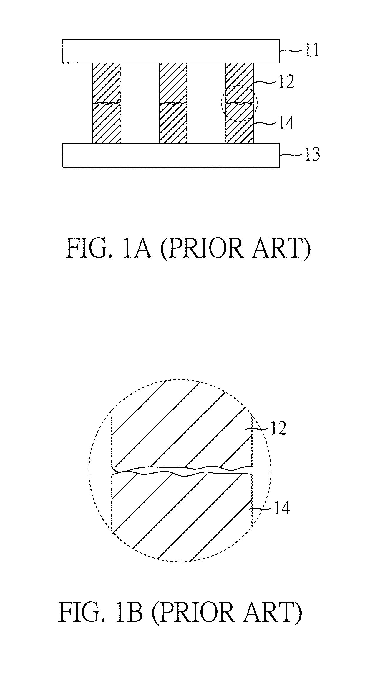
a technology of connecting elements and manufacturing methods, applied in the direction of electrical apparatus, semiconductor devices, semiconductor/solid-state device details, etc., can solve the problems of small grains without uniform stacking directions, components in circuit boards damaged, and the above thermo-compression process is not suitable for industrial manufacture, and achieve good adhesion
- Summary
- Abstract
- Description
- Claims
- Application Information
AI Technical Summary
Benefits of technology
Problems solved by technology
Method used
Image

Examples
example 1
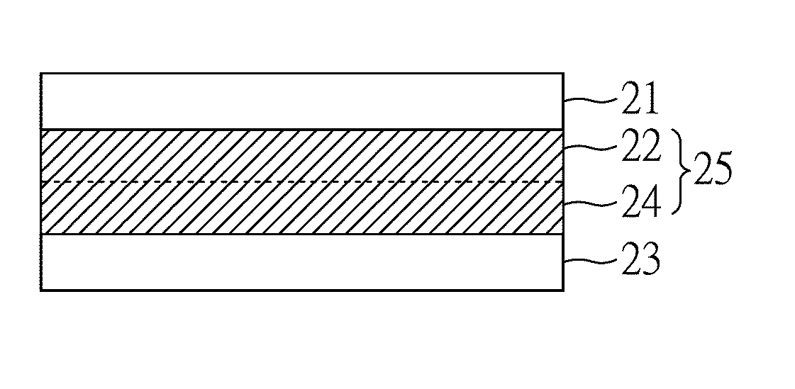
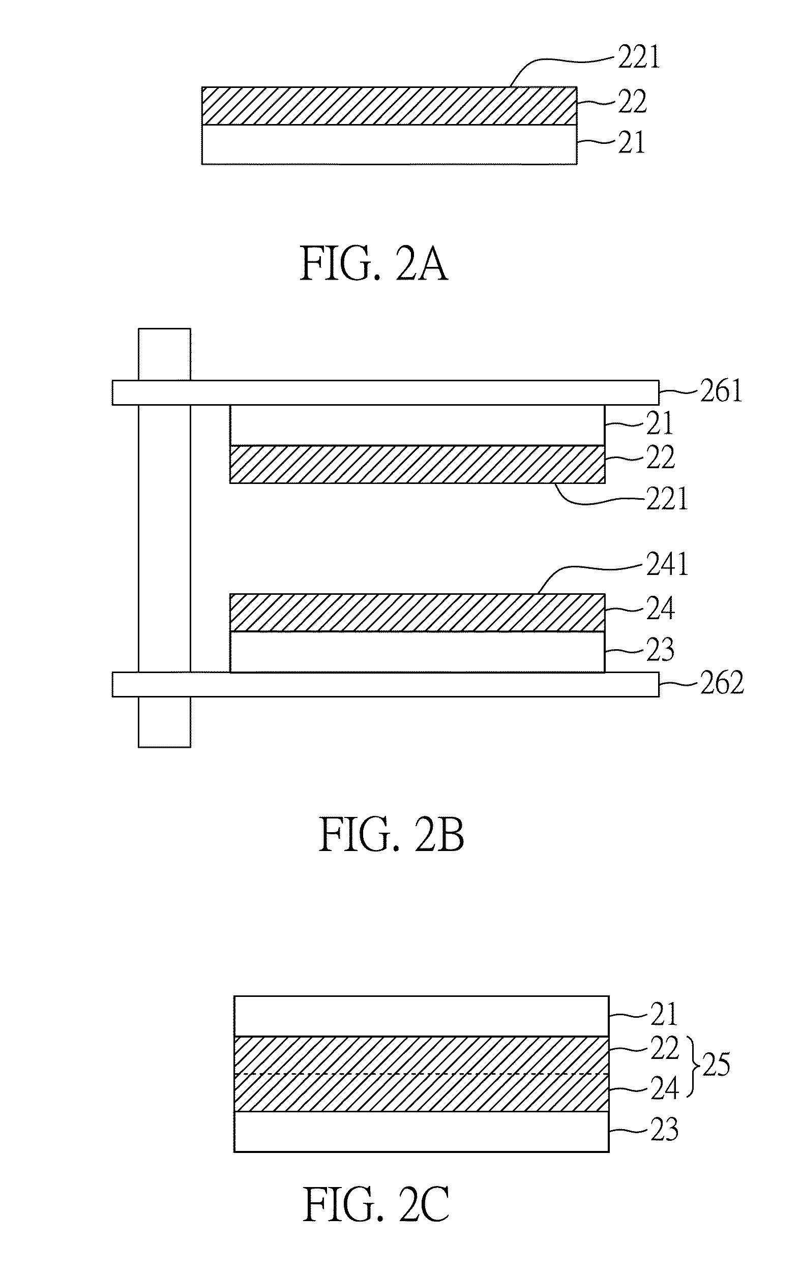
[0050]FIGS. 2A to 2C are cross-sectional views showing a process for manufacturing an electrical connection element having a twinned crystal copper layer of the present embodiment. The schematic view of a plating apparatus for forming the copper film in the present embodiment is shown in FIG. 3. A vertical view of an electron backscattered diffraction of the copper layer in the present embodiment is shown in FIG. 4, in which the ratio of the (111) surface is 100%. The focused ion beam cross-sectional view and a schematic view of the nanotwinned copper layer of the present embodiment are respectively shown in FIGS. 5A and 5B.
[0051]First, a first substrate 21 is provided, which is a wafer, as describes in FIG. 2A. In order to describe briefly, only the schematic view the first substrate 21 is exemplified, and circuits, active components, passive components or other components are not disclosed in the drawings.
[0052]Then, a plating process is performed on the first substrate 21 with th...
example 2
[0061]FIGS. 7A and 7B are cross-sectional views of a process for manufacturing the electrical connecting element having a nanotwinned copper of the present embodiment.
[0062]A plurality of the first copper films 22 and a plurality of the second copper films 24 are respectively formed on the first substrate 21 and the second substrate 23 in the present embodiment, as shown in FIGS. 7A and 7B. Herein, a plurality of the first copper films 22 and a plurality of the second copper films 24 can be respectively formed on the first substrate 21 and the second substrates 23 through the plating process described in Example 1 along with a lithography process. Herein, the first copper film 22 and the second copper film 24 respectively comprise a plurality of nanotwinned copper grains, the nanotwinned copper grains are composed by a plurality of nanotwinned copper, the nanotwinned copper grains are extended to the surface; and the [111] crystal axis is the axis vertical to the (111) surface. Thus...
example 3
[0066]The method for manufacturing a copper layer having (111) surface is shown as follows. First, a titanium layer (as an adhesion layer) with a thickness of 100 nm is deposited on the silicon wafer by a sputtering method, and then a copper layer having a (111) surface and a thickness of 200 nm is deposited on the titanium layer by a plating method. Herein, the copper layer can be prepared through the same plating process mentioned above. In the present embodiment, a silicon wafer with a copper layer having a (111) surface formed thereon is provided by the Amkor Technology Taiwan, INC. The ratio of the (111) surface can be controlled by forming different adhesion layer on the silicon wafer. Herein, 97% of the (111) surface can be obtained by using the titanium layer as an adhesion layer.
[0067]FIGS. 8A to 8C are cross-sectional views of a process for a manufacturing an electrical connecting element of the present embodiment; wherein the difference between the present embodiment and ...
PUM
| Property | Measurement | Unit |
|---|---|---|
| temperature | aaaaa | aaaaa |
| angle | aaaaa | aaaaa |
| temperature | aaaaa | aaaaa |
Abstract
Description
Claims
Application Information