Deposition of a high surface energy thin film layer for improved adhesion of group i-iii-vi2 solar cells

Inactive Publication Date: 2014-08-14
AERIS CAPITAL SUSTAINABLE IP
View PDF0 Cites 5 Cited by
  • Summary
  • Abstract
  • Description
  • Claims
  • Application Information

AI Technical Summary

Problems solved by technology

These electronic devices have been traditionally fabricated using silicon (Si) as a light-absorbing, semiconducting material in a relatively expensive production process.

Method used


Image

  • Deposition of a high surface energy thin film layer for improved adhesion of group i-iii-vi2 solar cells
  • Deposition of a high surface energy thin film layer for improved adhesion of group i-iii-vi2 solar cells
  • Deposition of a high surface energy thin film layer for improved adhesion of group i-iii-vi2 solar cells

Examples


Embodiment Construction

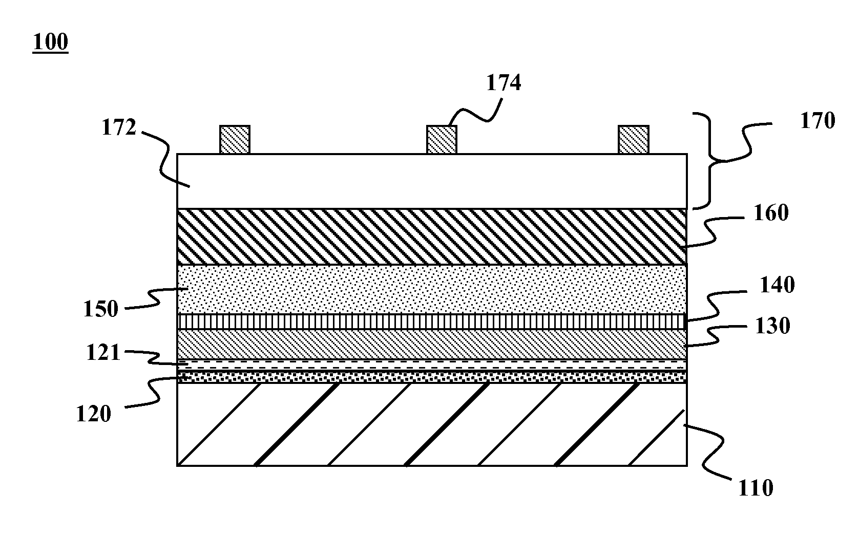
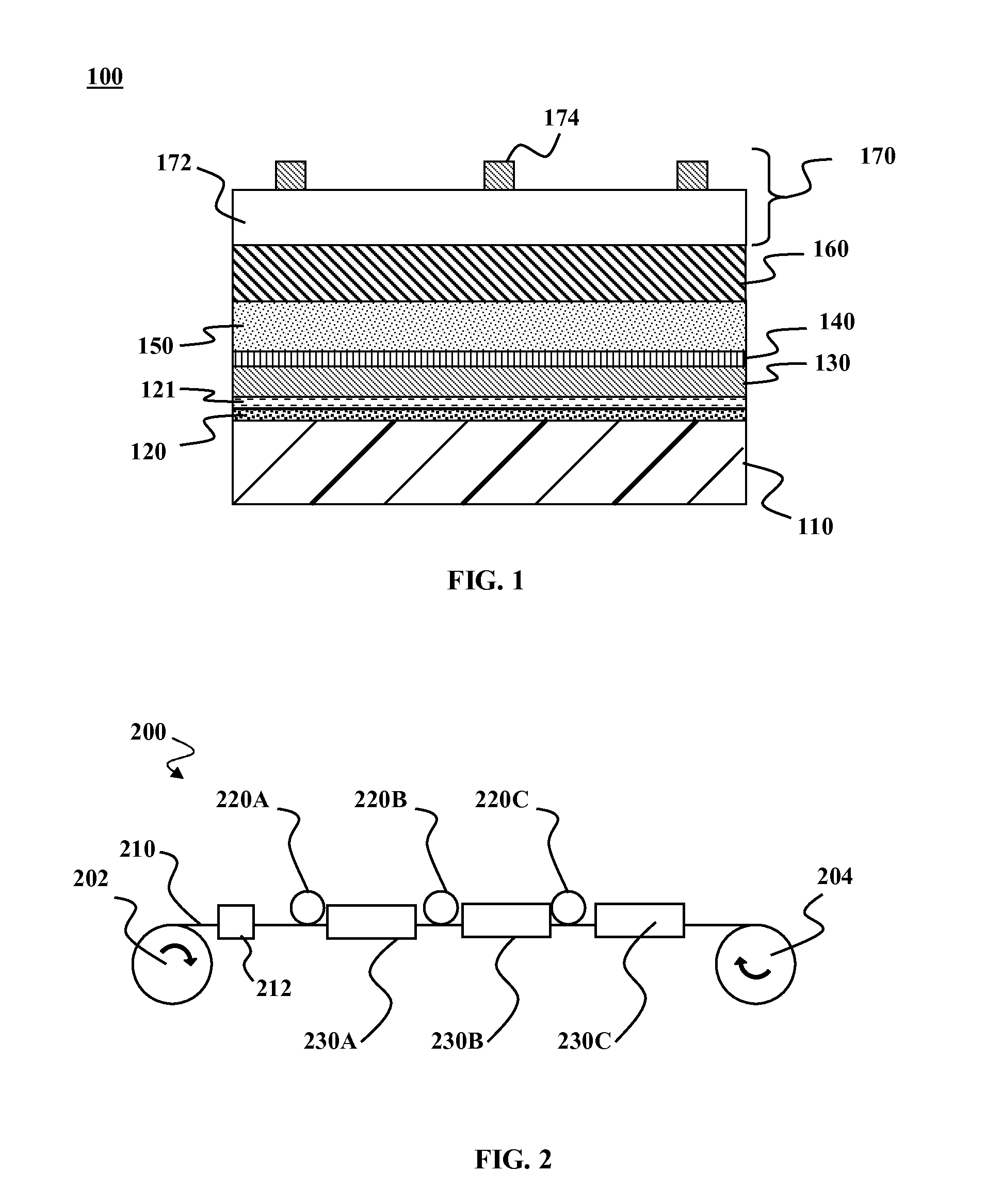
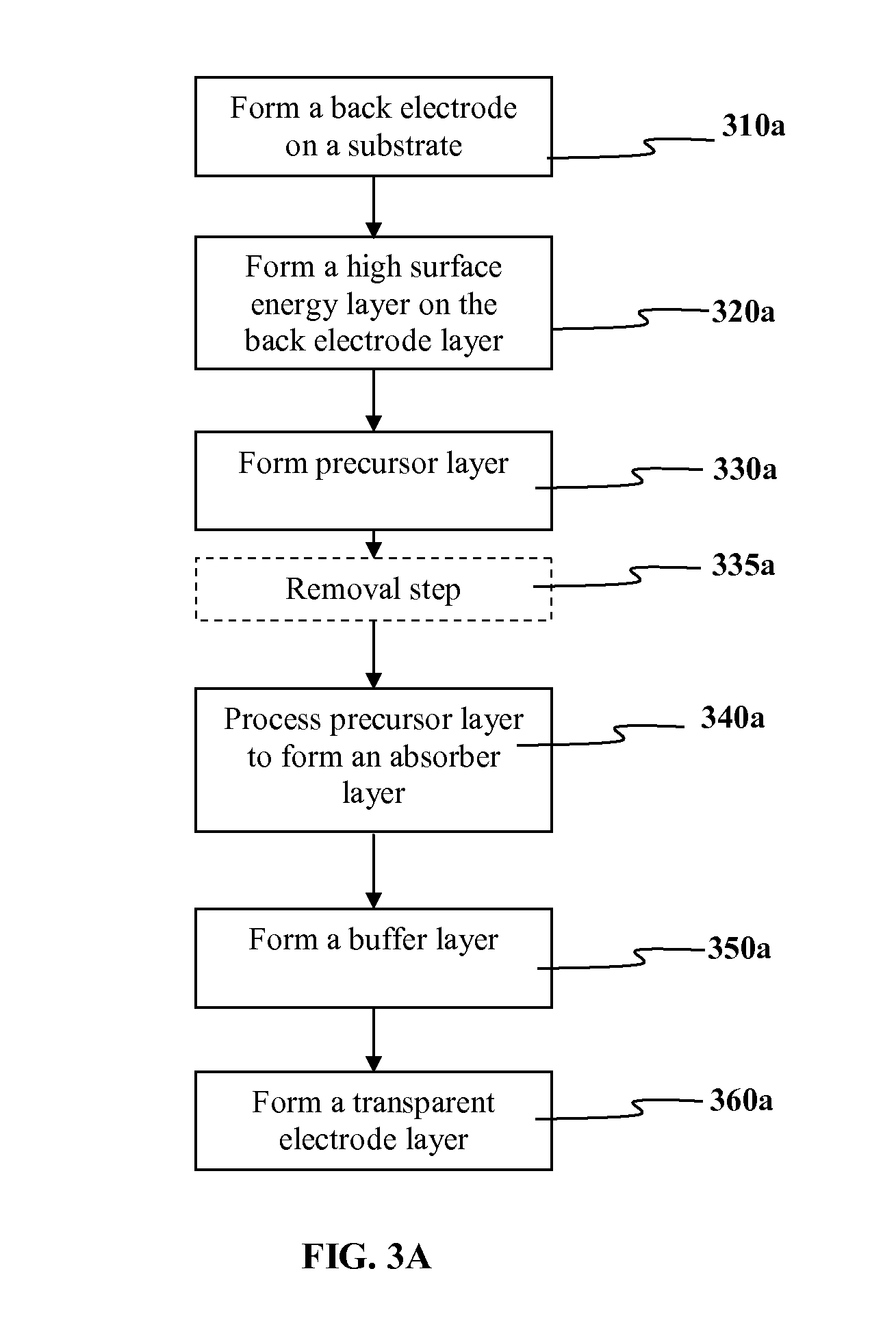
[0010]Although the following detailed description contains many specific details for the purposes of illustration, anyone of ordinary skill in the art will appreciate that many variations and alterations to the following details are within the scope of the invention. Accordingly, the aspects of the present disclosure described below are set forth without any loss of generality to, and without imposing limitations upon, the claims that follow this description.

[0011]“Optional” or “optionally” means that the subsequently described circumstance may or may not occur, so that the description includes instances where the circumstance occurs and instances where it does not. For example, if a device optionally contains a feature for an anti-reflective film, this means that the anti-reflective film feature may or may not be present, and thus, the description includes both structures wherein a device possesses the anti-reflective film feature and structures wherein the anti-reflective film fea...


PUM


Abstract

A thin film photovoltaic cell includes a light absorption layer of Group I-III-VI2 semiconductor materials and a high surface energy thin film layer that improves adhesion between the light absorption layer and an underlying electrode layer. The high surface energy thin film either replaces or is deposited on top of the back electrode to decrease the formation of voids at the back interface during absorber growth/deposition and thereby enabling a wider process window and improved cell efficiencies. It is emphasized that this abstract is provided to comply with the rules requiring an abstract that will allow a searcher or other reader to quickly ascertain the subject matter of the technical disclosure. It is submitted with the understanding that it will not be used to interpret or limit the scope or meaning of the claims.

Description

FIELD OF THE DISCLOSURE[0001]This disclosure relates generally to photovoltaic or solar cells. More particularly, it relates to fabrication of a thin film solar cell having a compound semiconductor material as a light absorber.BACKGROUND OF THE INVENTION[0002]Solar cells and solar modules convert sunlight into electricity. These electronic devices have been traditionally fabricated using silicon (Si) as a light-absorbing, semiconducting material in a relatively expensive production process. To make solar cells more economically viable, solar cell device architectures have been developed that can inexpensively make use of thin-film, preferably non-silicon, light-absorbing semiconductor materials with a chalcopyrite structure having excellent characteristics. Group I-III-VI2 semiconductor materials are usually used as light absorber for thin film solar cells, such as but not limited to copper indium gallium selenide (CIGS). Specifically, CIGS is a I-III-VI2 semiconductor material comp...

Claims


Application Information

Patent Timeline
Patent Type & Authority Applications(United States)
IPC IPC(8): H01L31/0216
CPCH01L31/02167H01L21/0237H01L21/02425H01L21/02491H01L21/02505H01L21/02568H01L21/02614H01L21/02628H01L31/022425H01L31/0322H01L31/03928H01L31/0749Y02E10/541
Inventor BROWN, GREGORYKIMBALL, GREGORYSTONE, PETER
Owner AERIS CAPITAL SUSTAINABLE IP
Why Eureka
Try Eureka