Gallium nitride semiconductor device with improved termination scheme

a technology of gallium nitride and semiconductor devices, which is applied in the direction of semiconductor devices, diodes, electrical devices, etc., can solve the problems of inconvenient provision of reliable guard rings such as p-type guard rings, lack of controllable manufacturing processes, and challenges in conventional methods of configuring and manufacturing gallium nitride (gan) based devices including schottky diodes as rectifying devices or devices for other functional applications, etc., to improve the effect of uniform density

Active Publication Date: 2014-08-14
ALPHA & OMEGA SEMICON INC
View PDF9 Cites 4 Cited by
  • Summary
  • Abstract
  • Description
  • Claims
  • Application Information

AI Technical Summary

Benefits of technology

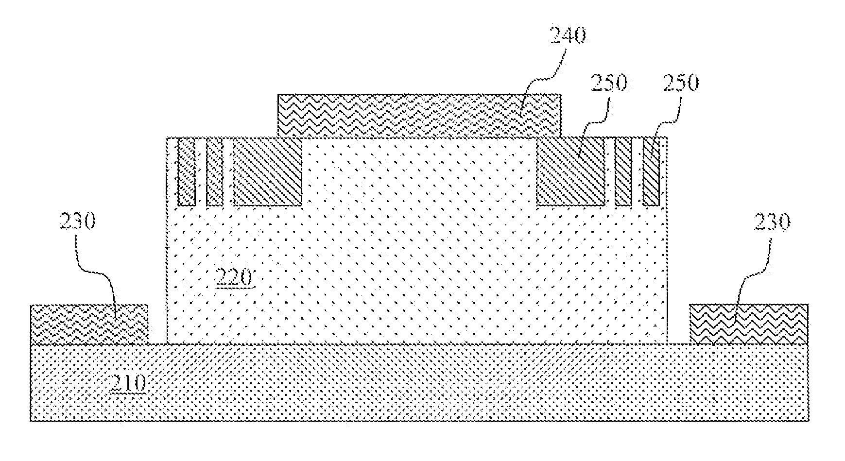
[0010]It is therefore an aspect of the present invention to provide a new and improved termination structure by forming the P-type guard rings near the edges of the device by applying an epitaxial growth process in the trenches to form the guard rings. The guard rings are formed with contr

Problems solved by technology

However, conventional methods of configuring and manufacturing gallium nitride (GaN) based devices including Schottky diodes as a rectifying device or devices for other functional applications are still challenged by a technical limitation of lacking controllable manufacturing processes to assure a reliable termination structure can be provided.
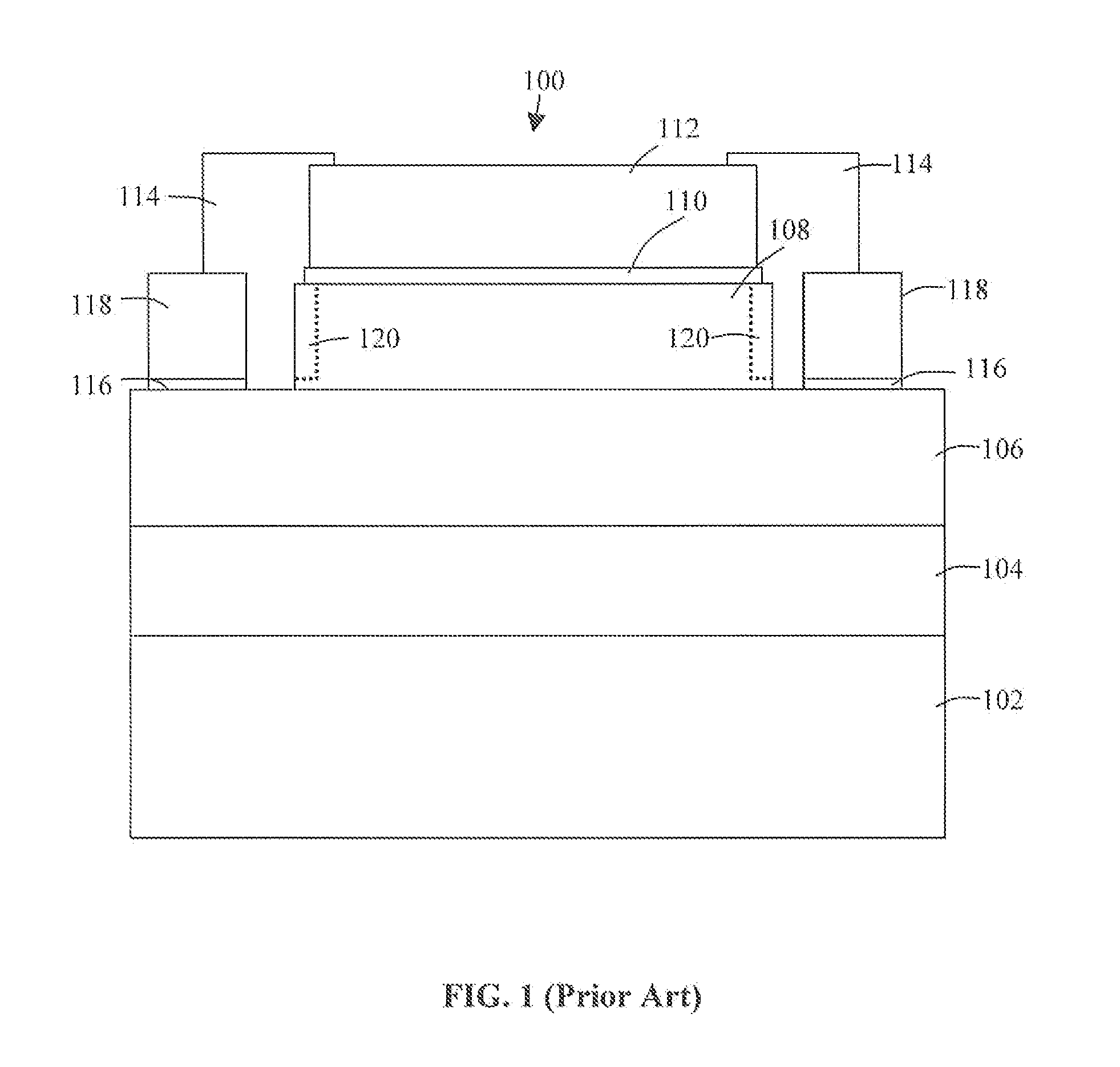
Due to the wide band-gap nature of the nitride semiconductor, reliable guard rings such as P-type guard rings cannot be conveniently provided by applying the conventional implant and diffusion processes commonly used with silicon based semiconductors.
However, for the nitride semiconductor device, an edge termination structure implemented with guard rings 120 as shown in FIG. 1, when formed by ion implantations followed by thermal activat

Method used


Image

  • Gallium nitride semiconductor device with improved termination scheme
  • Gallium nitride semiconductor device with improved termination scheme
  • Gallium nitride semiconductor device with improved termination scheme

Examples


Embodiment Construction

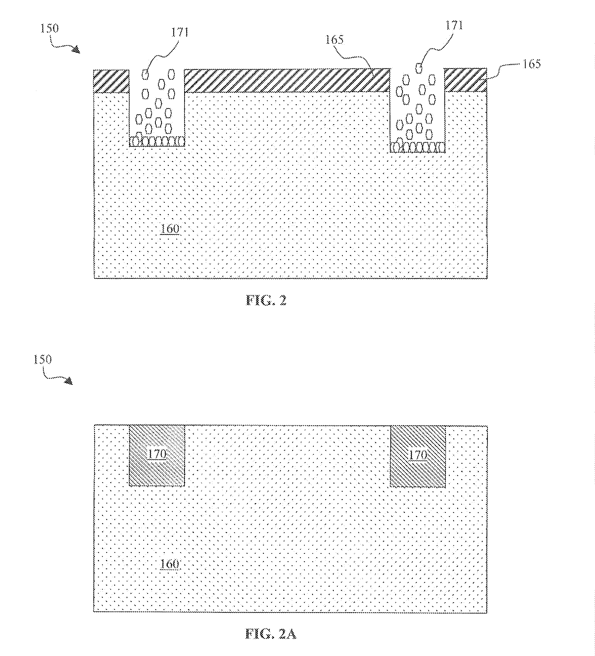
[0022]Refer to FIGS. 2 and 2A for a cross sectional view of a semiconductor device 150. The detailed configurations of the device 150 are not specifically shown here. The semiconductor device 150 includes an N-type Gallium nitride layer 160. The semiconductor device 150 further includes termination structures with p-type guard rings 170 formed by selective epitaxial growth 171. The epitaxial growth 171 is shown in FIG. 2, while the completed p-type guard rings are shown in FIG. 2A. By epitaxially growing the P-type GaN, the P-type guard rings 170 are formed having high quality and true P-type. As will be further described below the p-type guard rings are formed by applying a re-growth mask 165 to open trenches in the GaN layer 160. Then guard rings 170 are formed by epitaxial growth 171 in these trenches followed by removal of the regrowth mask 165 and a chemical mechanical planarization (CMP) process to planarize the p-type guard rings 170 complete the processes of forming the term...


PUM


Abstract

This invention discloses a gallium nitride based semiconductor power device disposed in a semiconductor substrate. The power device comprises a termination area disposed at a peripheral area of the semiconductor power device comprises a termination structure having at least a guard ring disposed in a trench filled with doped gallium-based epitaxial layer therein.

Description

[0001]This patent application is a Divisional application and claim the Priority Date of application of a co-pending application with a Ser. No. 12 / 589,911 filed by a common Inventor of this application on Oct. 30, 2009. The disclosures made in application Ser. No. 12 / 589,911 are hereby incorporated by reference.BACKGROUND OF THE INVENTION[0002]1. Field of the Invention[0003]The invention relates generally to the configurations and methods of manufacturing the semiconductor devices. More particularly, this invention relates to a gallium nitride (GaN)-based device implemented with new device configurations and manufacturing methods for providing reliable and high quality termination structure with guard rings formed by applying an epitaxial growth method.[0004]2. Description of the Prior Art[0005]The gallium nitride (GaN) based devices such as Schottky diodes have the advantage over silicon devices in achieving a high blocking voltage, while maintaining a low on-resistance using a sm...

Claims


Application Information

Patent Timeline
IPC IPC(8): H01L29/20H01L29/872
CPCH01L29/2003H01L29/872H01L29/0619H01L29/66212
Inventor ZHU, TINGGANG
Owner ALPHA & OMEGA SEMICON INC
Why Eureka
Try Eureka