Integrated optical structure comprising an optical isolator

a technology of optical isolators and integrated optical structures, which is applied in the field of optical isolators, can solve the problems of difficult integration of optical isolators into optical devices, high optical power loss of ferromagnetic metals, and difficult manufacture of optical isolators in commercial products, etc., and achieves the effect of facilitating the manufacture of optical isolators

Inactive Publication Date: 2014-09-04
ALCATEL LUCENT SAS
View PDF3 Cites 8 Cited by
  • Summary
  • Abstract
  • Description
  • Claims
  • Application Information

AI Technical Summary

Benefits of technology

[0012]It is a further purpose of the invention to disclose an integrated optical structure comprising an optical isolator whose performance is improved, particularly by a reduction in optical power losses, which contributes to a decrease in the SOA optical amplifier's power consumption.
[0013]It is a further purpose of the invention to disclose an integrated optical structure comprising an optical isolator that is easier and less expensive to manufacture.
[0031]Advantageously, the magneto-optical layer is etched in order to give it a structure that makes it possible to increase the magneto-optical effect.
[0035]the technology for producing the optical device is based on III-V on SOI hybrid integration, so the manufacturing of the isolator is much easier than in the prior art, and the optical isolator may thereby be used on silicon PIC photonic integrated circuits.

Problems solved by technology

Today, commercial products do not contain any optical isolators integrated into their chips.
This first type of optical isolator is hard to integrate into optical devices, as it requires multiple components whose integrated version is not yet available.
In this second sort of optical isolator, the ferromagnetic metals introduce high optical power losses, often greater than 20 dB, including in the incident direction.
In this case, there will be considerable optical power losses due both to the electrical contact layers, often made of an InGaAs, ternary semiconducting material, and to the electrical contact-conveying metallic layer, which is placed above the waveguide.
The step of removing material by etching turns out to be very difficult to carry out in this type of optical isolator.

Method used


Image

  • Integrated optical structure comprising an optical isolator
  • Integrated optical structure comprising an optical isolator
  • Integrated optical structure comprising an optical isolator

Examples


Embodiment Construction

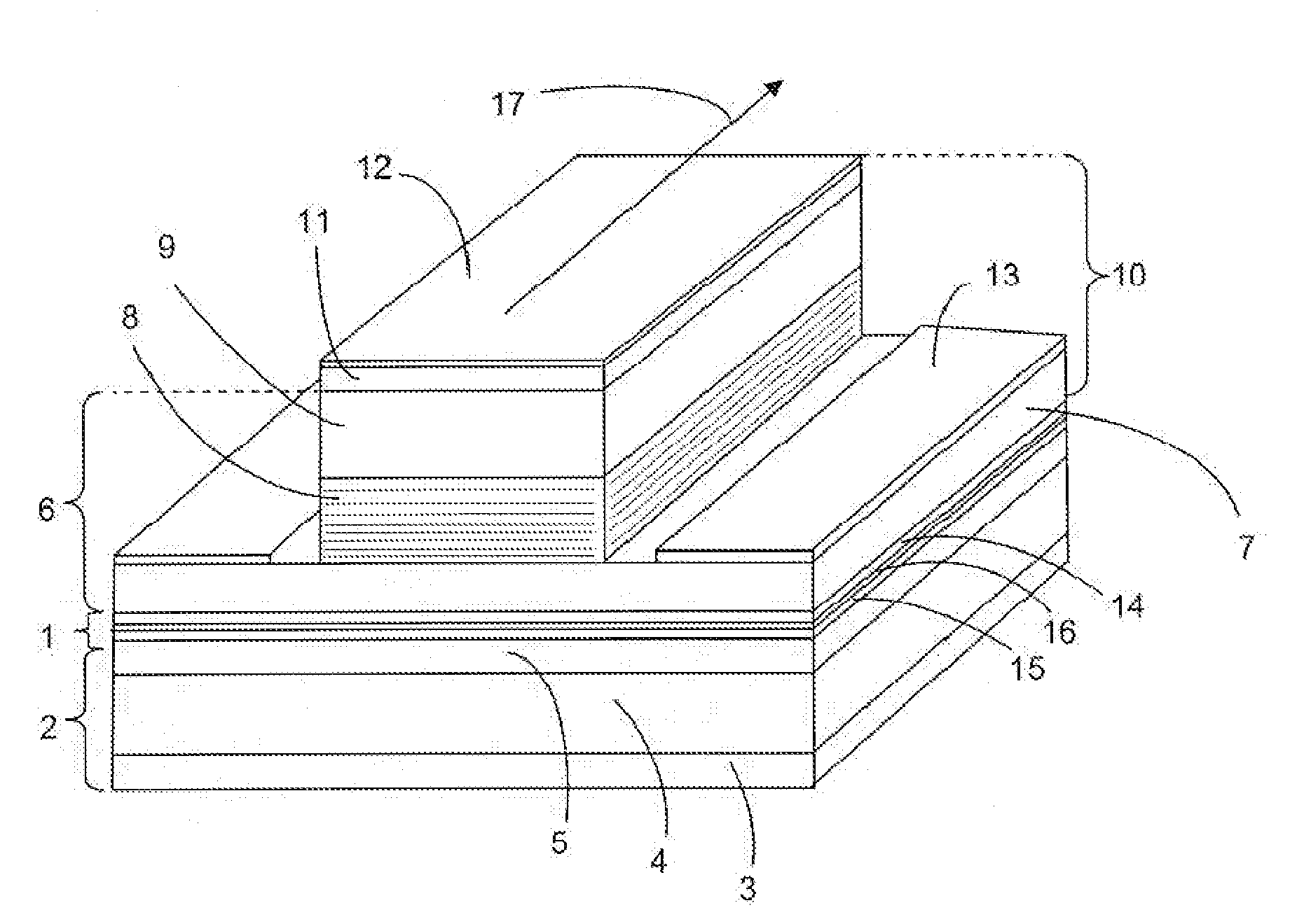
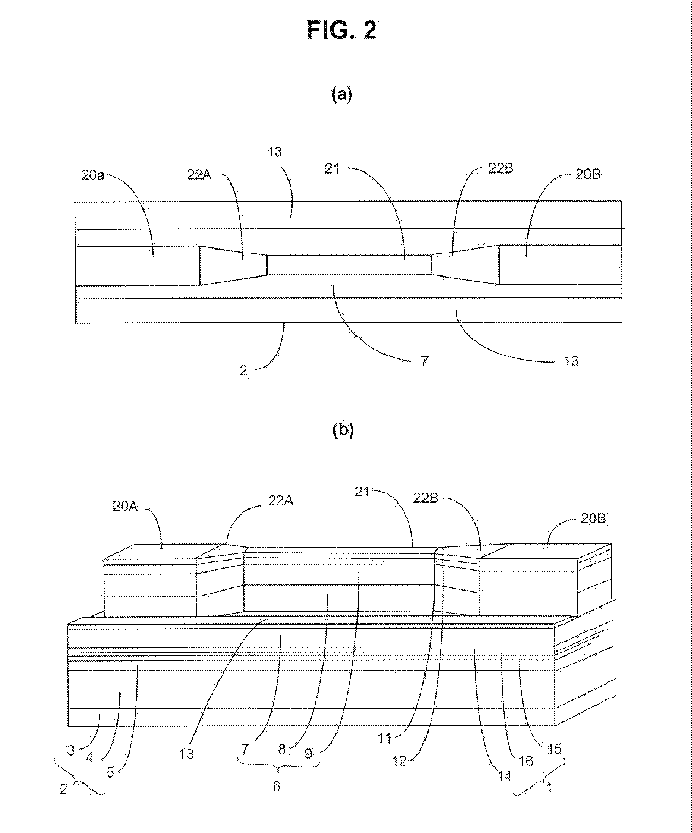
[0042]FIG. 1 depicts an integrated optical structure comprising an optical isolator created by the hybrid technology III-V on SOI. The SOI technology consists of inserting an electrically insulating layer of a silicon oxide SiOx, such as SiO2, between a semiconducting thin upper layer of silicon Si and a semiconducting thick lower layer of silicon Si, with the assembly constituting a SOI base.

[0043]The optical isolator 1 is integrated onto a SOI base 2 that comprises a crystalline silicon Si layer 3, or any other semiconducting substrate, covered by an insulating layer 4, for example one made of a silicon oxide SiOx like silica SiO2, topped with a second crystalline silicon Si layer 5. Typically, the thickness of the silicon layers is at most 0.5μm and that of the silicon oxide layer is about 2 μm.

[0044]The optical isolator 1 is associated with an optical waveguide 6 made of a stack of a semiconducting lower n-doped III-V layer 7, for example an indium phosphide InP based one, an ac...


PUM


Abstract

An integrated optical structure includes at least one optical isolator, having a magneto-optical layer, associated with at least one SOA optical amplifier having a waveguide having an n-doped semiconductor layer, a p-doped semiconductor layer, and an active area disposed between the n-doped semiconductor layer and the p-doped semiconductor layer. The optical isolator is disposed between an SOI base and the SOA optical amplifier's waveguide. The optical isolator's magneto-optical layer is disposed between a lower insulating layer and an upper insulating layer. The optical isolator's magneto-optical layer may be a layer of ferromagnetic metallic material, such as a Fe—Co metallic alloy, or a magnetic oxide layer. An optical device includes at least one integrated optical structure.

Description

CROSS-REFERENCE[0001]This application is based on French Patent Application No. 11,59,501 filed on Oct. 20, 2011, the disclosure of which is hereby incorporated by reference thereto in its entirety, and the priority of which is hereby claimed under 35 U.S.C. §119.BACKGROUND[0002]The present invention pertains to an optical isolator intended to be integrated into optical devices, such as optoelectronic components, and, in particular, photonic integrated circuits, or PICs. These optical devices are used mainly in the field of high-speed digital telecommunications. The invention also extends to the method for manufacturing such an optical isolator.[0003]An optical isolator is a nonreciprocal passive device that has high attenuation in one direction and low attenuation in the opposite direction; it makes it possible to transmit light in only one direction, but prevents light from propagating in an opposite direction. For this reason, optical isolators are essential elements for eliminat...

Claims


Application Information

Patent Timeline
Patent Type & Authority Applications(United States)
IPC IPC(8): H01S5/00
CPCH01S5/0064B82Y20/00Y10S977/755G02F1/0955H01S5/026H01S5/50H01S5/021H01S5/1014H01S5/02325G02B2006/12157G02B2006/12085
Inventor DUAN, GUANG-HUABRILLOUET, FRANCOISGENTNER, JEAN-LOUIS
Owner ALCATEL LUCENT SAS
Why Eureka
Try Eureka