Method For Producing Optical Member And Use Of UV-Curable Resin Composition Therefor
- Summary
- Abstract
- Description
- Claims
- Application Information
AI Technical Summary
Benefits of technology
Problems solved by technology
Method used
Image

Examples
first embodiment
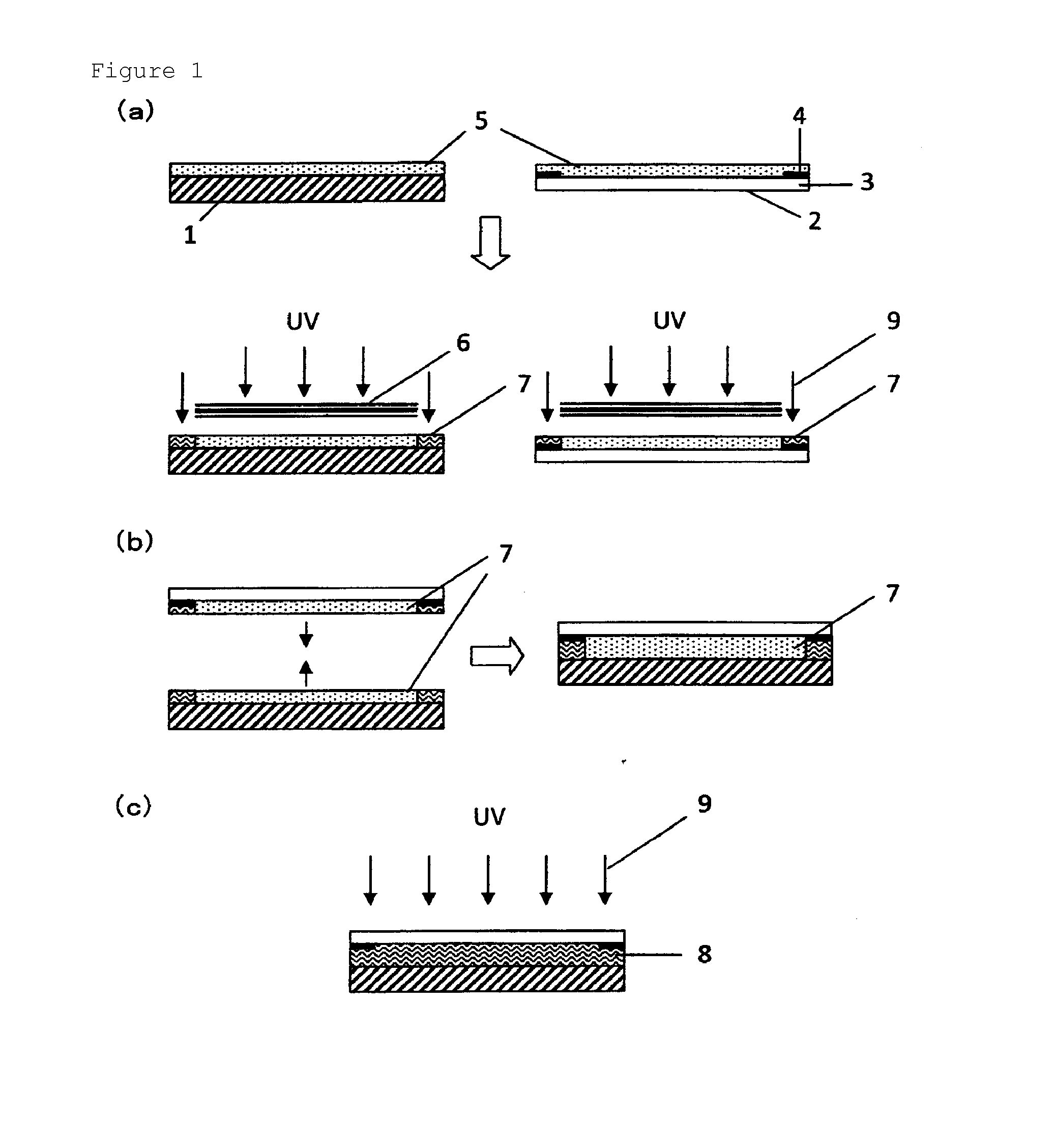
[0075]FIGS. 1(a) to 1(c) are process diagrams illustrating the first embodiment of the method of producing an optical member using an ultraviolet curable resin composition according to the invention.
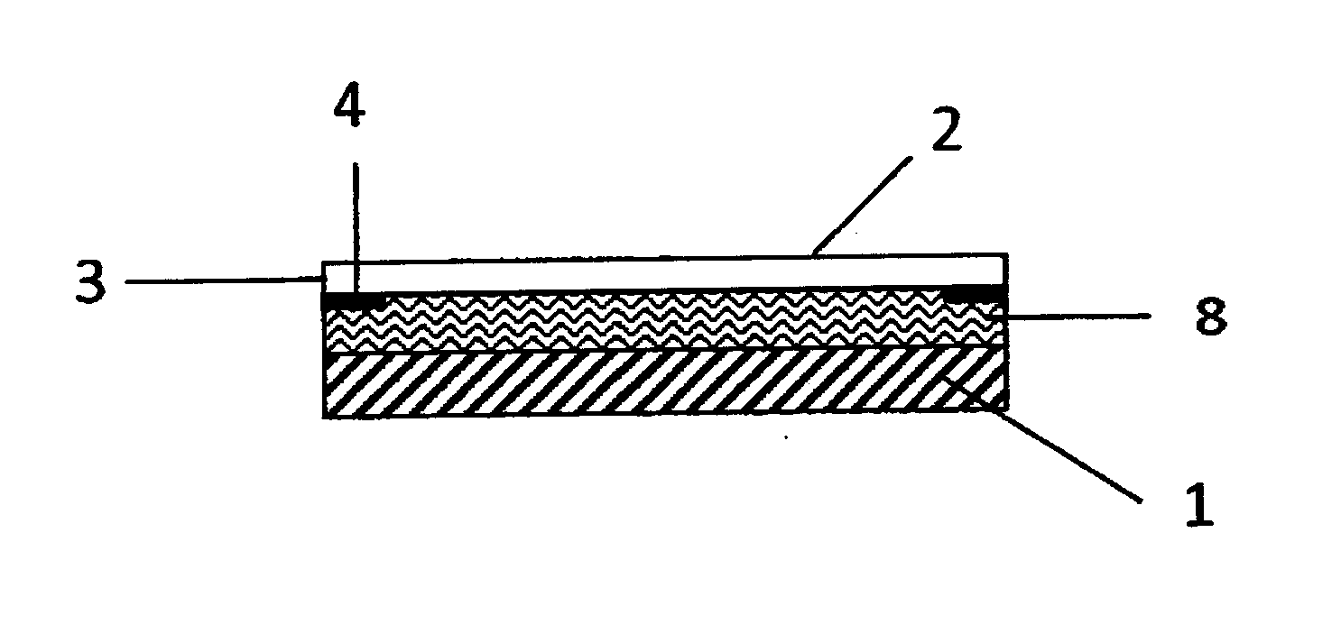
[0076]This first embodiment is a method of obtaining an optical member (a liquid crystal display unit having a light shielding portion) by bonding a liquid crystal display unit 1 to a transparent substrate 2 having a light shielding portion.
[0077]The liquid crystal display unit 1 is a liquid crystal display unit prepared by enclosing a liquid crystal material between a pair of substrates having an electrode formed thereon and then equipping the pair of substrates with a polarizing plate, a driving circuit, a signal input cable, and a backlight unit.
[0078]The transparent substrate 2 having a light shielding portion is a transparent substrate prepared by forming a light shielding portion 4 of black frame shape on the surface of the bonding surface of a transparent substrate 3 such as a gla...
second embodiment
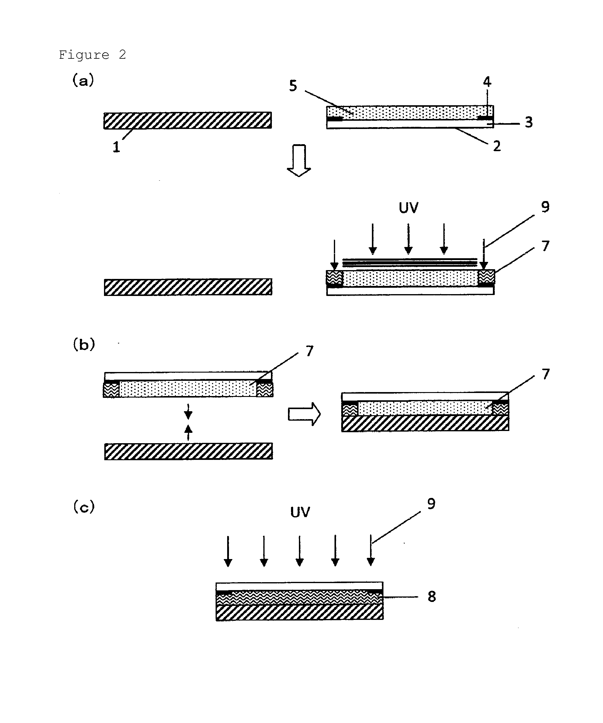
[0099]FIGS. 2(a) to 2(c) are process diagrams illustrating the second embodiment of the method of producing an optical member using an ultraviolet curable resin composition according to the invention.
[0100]Meanwhile, the same reference numerals in the figures refer to the same elements as the constitutional elements in the first embodiment described above, and the explanation thereof will not be repeated here.
[0101](Process 1)
[0102]First, as illustrated in FIG. 2 (a), an ultraviolet curable resin composition is coated on the surface provided with a light shielding portion 4 of a transparent substrate 2 having a light shielding portion. Thereafter, a coating layer 7 of the ultraviolet curable resin composition having a light shielded region at the time of bonding cured is obtained by irradiating the light shielded region at the time of bonding with ultraviolet rays. Here, the region exposed to light at the time of bonding is masked with an ultraviolet shielding plate 6, whereby the r...
third embodiment
[0108]The optical member of the invention can be produced according to the third embodiment modified as follows in addition to the first embodiment and the second embodiment.
[0109](Process 1)
[0110]First, an ultraviolet curable resin composition is coated on the display surface of a liquid crystal display unit 1, and then a coating layer 7 of the ultraviolet curable resin composition having a light shielded region at the time of bonding cured is obtained by irradiating the light shielded region at the time of bonding with ultraviolet rays. Here, the region exposed to light at the time of bonding is masked with an ultraviolet shielding plate 6, whereby the resin composition in the region exposed to light is not cured when irradiation with ultraviolet rays is performed.
[0111](Process 2)
[0112]Next, a liquid crystal display unit 1 and the transparent substrate 2 having a light shielding portion are bonded to each other in the form that the coating layer 7 of the liquid crystal display un...
PUM
| Property | Measurement | Unit |
|---|---|---|
| Percent by mass | aaaaa | aaaaa |
| Percent by mass | aaaaa | aaaaa |
| Percent by mass | aaaaa | aaaaa |
Abstract
Description
Claims
Application Information
 - R&D
- Intellectual Property
- Life Sciences
- Materials
- Tech Scout
- Unparalleled Data Quality
- Higher Quality Content
- 60% Fewer Hallucinations
Browse by: Latest US Patents, China's latest patents, Technical Efficacy Thesaurus, Application Domain, Technology Topic, Popular Technical Reports.
© 2025 PatSnap. All rights reserved.Legal|Privacy policy|Modern Slavery Act Transparency Statement|Sitemap|About US| Contact US: help@patsnap.com