Wafer-to-wafer oxide fusion bonding

a technology of fusion bonding and wafers, applied in the direction of electrical equipment, chemistry equipment and processes, lamination ancillary operations, etc., can solve the problems of reducing yield, cracking, and delamination of the edge zone of the fusion bonding, and reducing the usable space on the wafer

Inactive Publication Date: 2014-09-18
IBM CORP
View PDF0 Cites 37 Cited by
  • Summary
  • Abstract
  • Description
  • Claims
  • Application Information

AI Technical Summary

Problems solved by technology

One of the challenges for oxide-oxide fusion bonding is chipping, cracking, and delamination at the wafer edge zone during thinning of wafer stacks caused by bonding voids and defects.
This is typically handled by performing an edge trimming step to remove the defective edge zone after bonding or after preliminary thinning, which results in reducing usable space on the wafer and reducing yield.
If the final device comprises multiple layers, additional edge trimming after each wafer-to-wafer bonding and / or thinning may further reduce yield.

Method used


Image

  • Wafer-to-wafer oxide fusion bonding
  • Wafer-to-wafer oxide fusion bonding
  • Wafer-to-wafer oxide fusion bonding

Examples


Embodiment Construction

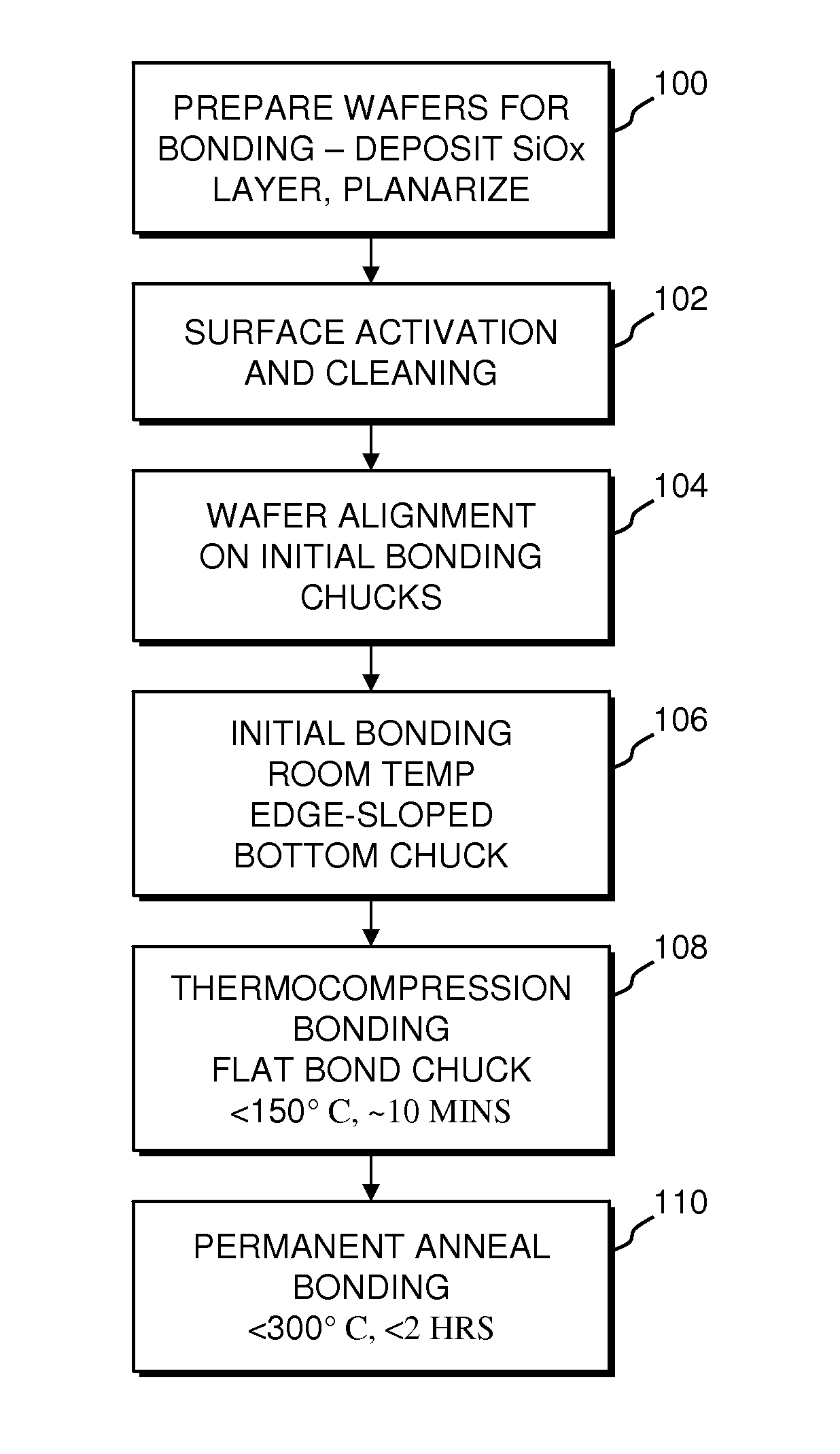
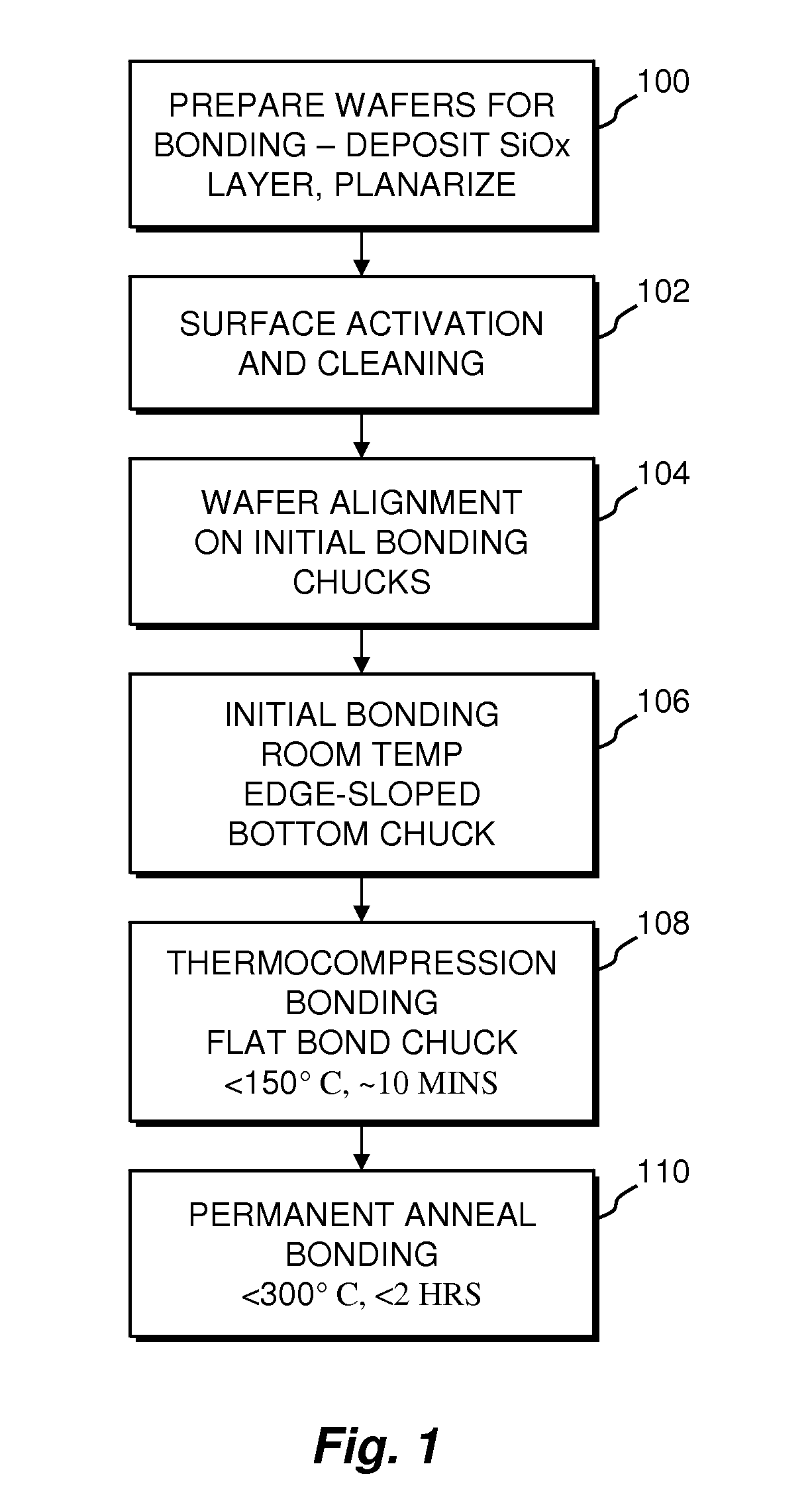
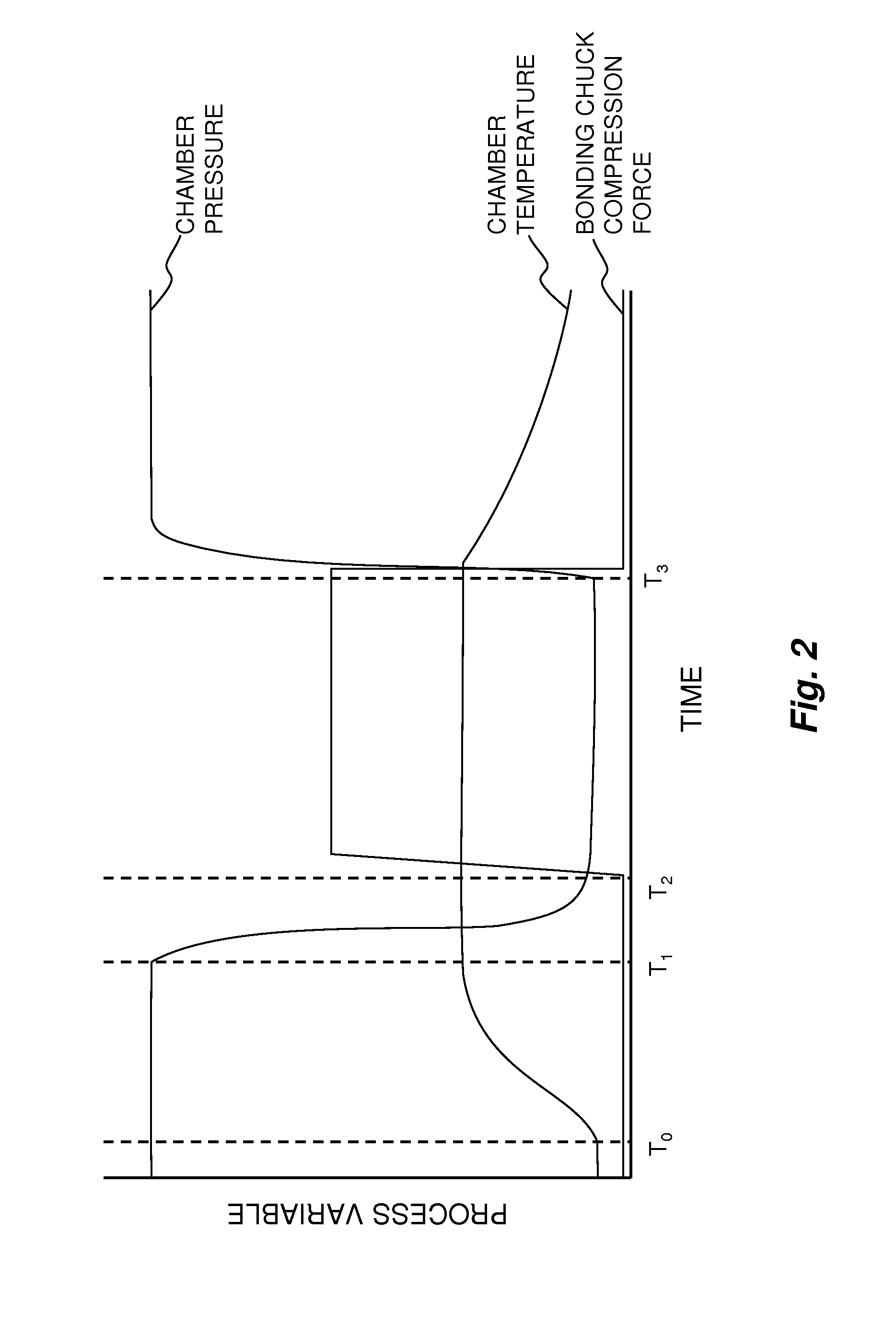
[0018]Embodiments of the invention described in detail herein are directed to a process that improves oxide-oxide fusion bonding to reduce or eliminate edge chipping and cracking by enhancing the edge zone bonding at the wafer edge. In the disclosed embodiments, a low temperature thermocompression step is performed following the alignment and initial bonding steps, and before the permanent bonding anneal step. As further disclosed, the thermocompression step may be performed with the aid of a bonding chuck that, among its other possible advantages, operates to improve the oxide-oxide fusion bonding to reduce or eliminate edge chipping and cracking by enhancing the edge zone bonding.

[0019]It should be appreciated that although specific wafer substrate bonding process flows are described herein, such descriptions are exemplary only, and that the principles disclosed are also applicable to various types of conductive materials, dielectric and adhesive interface materials, and multiple ...


PUM

PropertyMeasurementUnit
widthaaaaaaaaaa
widthaaaaaaaaaa
radial annular widthaaaaaaaaaa

Abstract

Oxide-oxide fusion bonding of wafers that includes performing a van der Waals force bonding process with a chuck having at least a flat central zone and an outer annular zone lower than the central zone, an edge portion of a mounted wafer is biased towards the outer annular zone. The van der Waals bonding wave is disrupted at the outer annular zone, causing an edge gap. A thermocompression bonding process is performed that includes heating the bonded wafers to a temperature sufficient to initiate condensation of silanol groups between the bonding surfaces, reducing the atmospheric pressure to cause degassing from between the wafers, applying a compression force to the wafers with flat chucks so as to substantially eliminate the edge gap, and performing a permanent anneal bonding process.

Description

FIELD OF THE INVENTION[0001]The present invention relates generally to the field of semiconductor device manufacturing, and more particularly to a process and apparatus for the bonding together of semiconductor substrates.CROSS-REFERENCE TO RELATED APPLICATIONS[0002]The present application is related to U.S. patent application Ser. No. ______ filed on Mar. 14, 2013, entitled “Wafer-to-Wafer Fusion Bonding Chuck” having IBM docket no. FIS920120309US1.BACKGROUND OF THE INVENTION[0003]Semiconductor devices are typically produced in arrays on wafer substrates ranging from 1 to 18 inches in diameter. The devices are then separated into individual devices or dies that are packaged to allow practical macro-level connection of the devices in the context of a larger circuit. As the requirements for chip density and smaller packaging form factors increase, advances have been made in three-dimensional integration of circuits. In this technology, devices are stacked, and bonded in the vertical ...

Claims


Application Information

Patent Timeline
Patent Type & Authority Applications(United States)
IPC IPC(8): H01L21/02
CPCH01L21/02H01L21/2007H01L21/67092
Inventor LIN, WEIPRIYADARSHINI, DEEPIKASKORDAS, SPYRIDONVO, TUAN A.
Owner IBM CORP
Why Eureka
Try Eureka