
Oxygen Controlled PVD Aluminum Nitride Buffer for Gallium Nitride-Based Optoelectronic and Electronic Devices

a technology of gallium nitride and aluminum nitride, which is applied in the field of group iiinitride materials, can solve the problems of difficult growth or depositing on foreign substrates, difficult to achieve high-quality surface preservation of select films, and difficult to grow or deposit on foreign substrates, etc., and achieves low rate of rise and high base vacuum

Active Publication Date: 2014-09-18
APPLIED MATERIALS INC
View PDF11 Cites 24 Cited by
  • Summary
  • Abstract
  • Description
  • Claims
  • Application Information

AI Technical Summary

Benefits of technology

This patent describes a chamber that can create a layer of aluminum nitride (AlN) for use in electronic and optoelectronic devices. The chamber has a high vacuum and low temperature rate of rise to ensure a stable and uniform layer of AlN. It also has a full face erosion magnetron cathode that ensures consistent target erosion and deposition of AlN across carriers. The chamber also has a process kit and gas flow design that ensures a uniform distribution of process gases, including oxygen-containing gas, for a uniform composition of AlN.

Problems solved by technology

Often, group III-V materials are difficult to grow or deposit on foreign substrates (known as heteroepitaxy) without the formation of defects or cracks.
For example, high quality surface preservation of select films, e.g. a gallium nitride film, is not straightforward in many applications using stacks of material layers fabricated sequentially.
However, group III-V materials are often sensitive to process conditions and care must be taken to avoid such conditions at particular periods of the fabrication process.
Avoiding interaction of a sensitive group III-V film with potential damaging conditions, however, is also not straightforward in many applications.

Method used


Image

  • Oxygen Controlled PVD Aluminum Nitride Buffer for  Gallium Nitride-Based Optoelectronic and Electronic Devices
  • Oxygen Controlled PVD Aluminum Nitride Buffer for  Gallium Nitride-Based Optoelectronic and Electronic Devices
  • Oxygen Controlled PVD Aluminum Nitride Buffer for  Gallium Nitride-Based Optoelectronic and Electronic Devices

Examples


Embodiment Construction

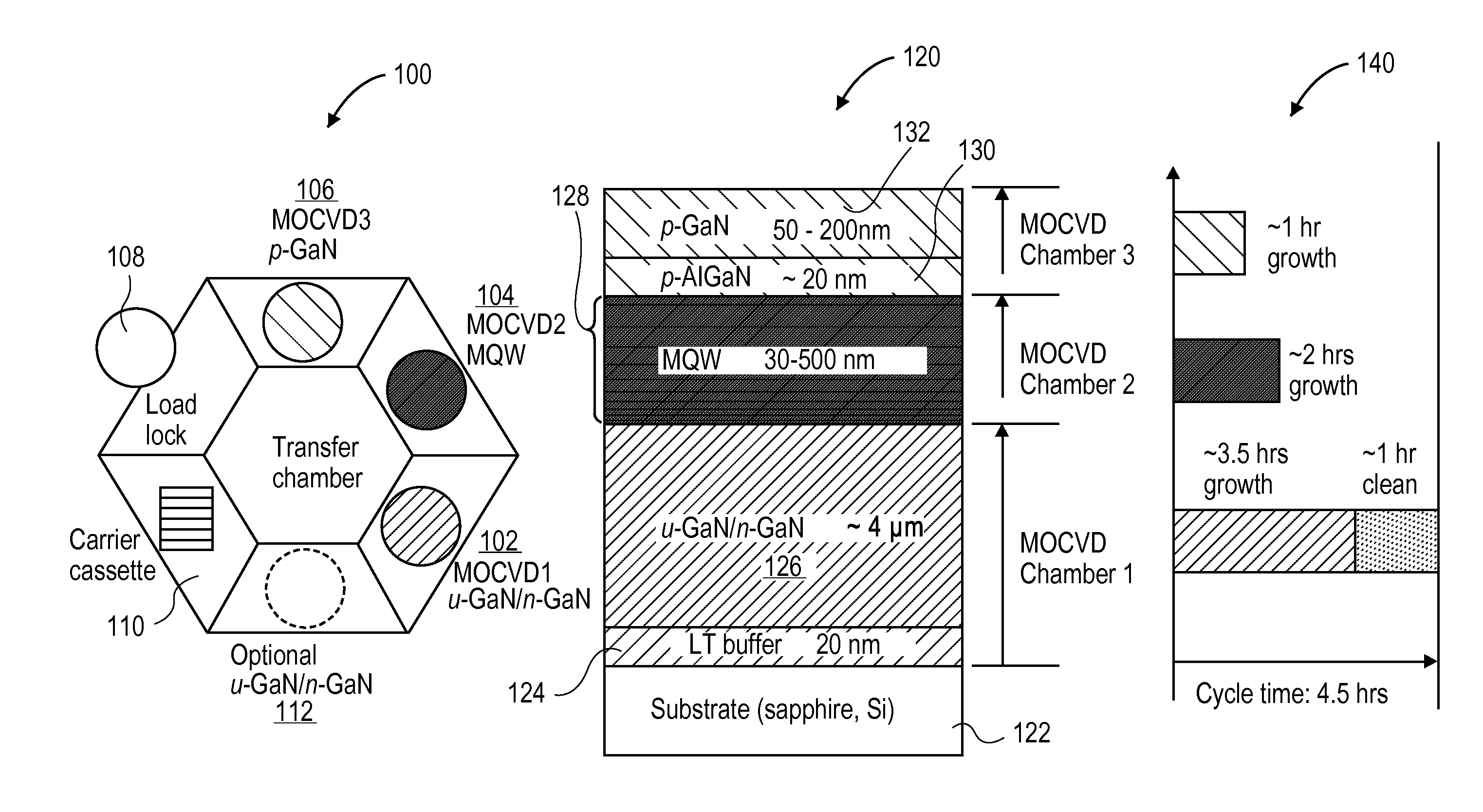
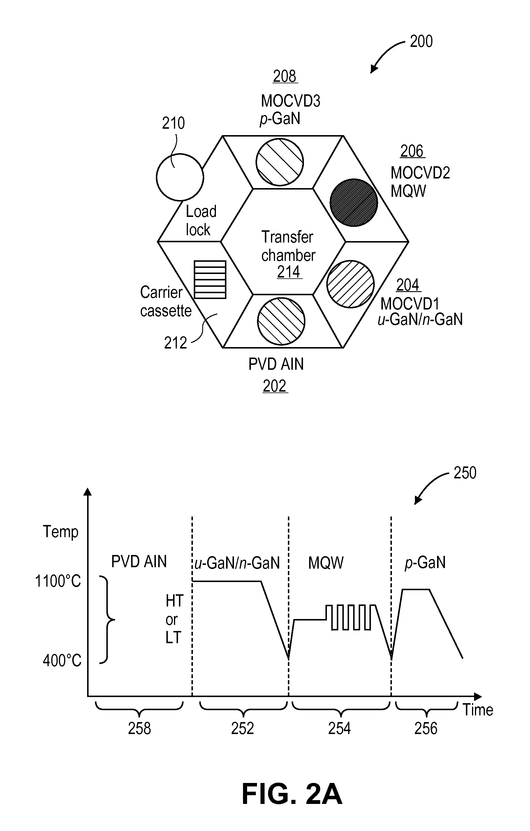
[0020]The fabrication of gallium nitride-based optoelectronic or electronic devices with physical vapor deposition (PVD) formed aluminum nitride (AlN) buffer layers is described. In the following description, numerous specific details are set forth, such as process chamber configurations and material regimes, in order to provide a thorough understanding of embodiments of the present invention. It will be apparent to one skilled in the art that embodiments of the present invention may be practiced without these specific details. In other instances, well-known features, such as specific diode configurations, are not described in detail in order to not unnecessarily obscure embodiments of the present invention. Furthermore, it is to be understood that the various embodiments shown in the Figures are illustrative representations and are not necessarily drawn to scale. Additionally, other arrangements and configurations may not be explicitly disclosed in embodiments herein, but are still...


PUM

PropertyMeasurementUnit
temperatureaaaaaaaaaa
temperaturesaaaaaaaaaa

Abstract

Oxygen controlled PVD AlN buffers for GaN-based optoelectronic and electronic devices is described. Methods of forming a PVD AlN buffer for GaN-based optoelectronic and electronic devices in an oxygen controlled manner are also described. In an example, a method of forming an aluminum nitride (AlN) buffer layer for GaN-based optoelectronic or electronic devices involves reactive sputtering an AlN layer above a substrate, the reactive sputtering involving reacting an aluminum-containing target housed in a physical vapor deposition (PVD) chamber with a nitrogen-containing gas or a plasma based on a nitrogen-containing gas. The method further involves incorporating oxygen into the AlN layer.

Description

CROSS-REFERENCE TO RELATED APPLICATIONS[0001]This application claims the benefit of U.S. Provisional Application No. 61 / 785,128, filed Mar. 14, 2013, the entire contents of which are hereby incorporated by reference herein.BACKGROUND[0002]1) Field[0003]Embodiments of the present invention pertain to the field of group III-nitride materials and, in particular, to the fabrication of gallium nitride-based optoelectronic or electronic devices with physical vapor deposition (PVD) formed aluminum nitride buffer layers.[0004]2) Description of Related Art[0005]Group III-V materials are playing an ever increasing role in the semiconductor and related, e.g. light-emitting diode (LED), industries. Often, group III-V materials are difficult to grow or deposit on foreign substrates (known as heteroepitaxy) without the formation of defects or cracks. For example, high quality surface preservation of select films, e.g. a gallium nitride film, is not straightforward in many applications using stack...

Claims


Application Information

Patent Timeline
Patent Type & Authority Applications(United States)
IPC IPC(8): H01L33/00H01L31/18H01J37/34H01L29/20
CPCH01L33/007H01L33/12H01L31/1856H01L29/2003H01J37/3405H01J37/32467H01J37/32724H01J37/347Y02E10/544H01L33/0075
Inventor ZHU, MINGWEIPATIBANDLA, NAG B.WANG, RONGJUNDIEHL, DANIEL LEEAGRAWAL, VIVEKSUBRAMANI, ANANTHA
Owner APPLIED MATERIALS INC
Learn More