
Method of forming dual gate oxide

Inactive Publication Date: 2014-09-18
SHANGHAI HUALI MICROELECTRONICS CORP
View PDF6 Cites 0 Cited by
  • Summary
  • Abstract
  • Description
  • Claims
  • Application Information

AI Technical Summary

Benefits of technology

The present invention proposes a way to prevent defects in photoresist during a wet etching process. This method makes the photoresist resistant to the acidic solution while not affecting production speed.

Problems solved by technology

However, accompanying with its etching effect on the silicon oxide film 3, the acidic solution also influences the photoresist 4 and causes defects therein, mainly including photoresist residues and silicon carbide (SiC) deposits.
However, these photoresist-defect prevention methods of the prior art each suffer from a number of deficiencies.
One deficiency is that, in the baking method, the baking step should not be performed at an excessively high temperature for too long, otherwise, the photoresist pattern will deform, thus adversely affecting production throughput.
On the other hand, limited baking temperature and duration may lead to the baked photoresist having an insufficient density to resist the encroachment of the acidic solution.
Another deficiency lies in that the surface-curing method requires a UV or plasma treatment after the photolithographic process, which needs to be performed on other equipment and hence leads to disadvantages, such as increasing process cost, elongating production cycle and reducing production throughput.

Method used


Image

  • Method of forming dual gate oxide
  • Method of forming dual gate oxide
  • Method of forming dual gate oxide

Examples


embodiment 1

[0026]This embodiment provides a method, of forming a dual gate oxide described in detail below, wherein a dual gate oxide refers to a gate oxide layer having at least two portions with different thicknesses.

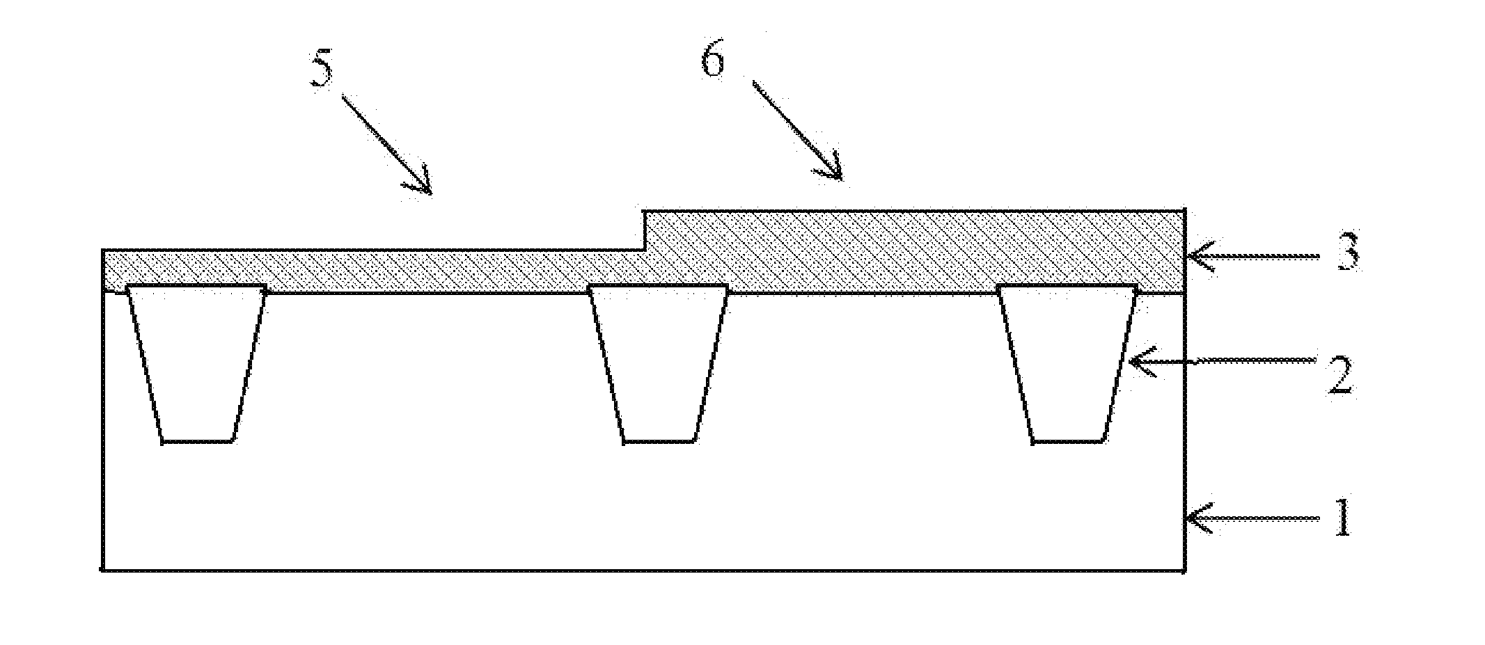
[0027]Referring to FIG. 5a, in the method, photoresist 4 is first coated over a silicon oxide film 3 deposited on a silicon substrate 1 in which a number of shallow trench isolation (STI) structures 2 have been formed. The photoresist can be used include those for use in I-line, 248 nm, 193 nm and extreme ultraviolet (EUV) photolithographic processes.

[0028]Next, as shown in FIG. 5b, the photoresist 4 is exposed and developed, thereby exposing a portion of the underlying silicon oxide film 3 for receiving a subsequent wet etching process, referred to hereinafter as “the first silicon oxide region” indicated at 5, with the rest portion of the silicon oxide film 3, referred to hereinafter as “the second silicon oxide region” indicated at 6, being protected by the remaining photores...

embodiment 2

[0039]This embodiment provides another method of forming a dual gate oxide described in detail below, wherein a dual gate oxide refers to a gate oxide layer having at least two portions with different thicknesses.

[0040]Referring to FIG. 6a, in the method, photoresist 4 is coated over a silicon oxide film 3 deposited on a silicon substrate 1 in which a number of shallow trench isolation (STI) structures 2 have been formed. The photoresist can be used include those for use in I-line, 248 nm, 193 nm and extreme ultraviolet (EUV) photolithographic processes.

[0041]Next, as shown in FIG. 6b, the photoresist 4 is exposed and developed in a developing apparatus, thereby exposing a portion of the underlying silicon oxide film 3 for receiving a subsequent wet etching process, referred to hereinafter as “the first silicon oxide region” indicated at 5, with the rest portion of the silicon oxide film 3, referred to hereinafter as “the second silicon oxide region” indicated at 6, being protected ...


PUM


Abstract

A method of forming a dual gate oxide is disclosed which includes: providing a silicon substrate; depositing a first silicon oxide film over the silicon substrate; coating a photoresist over the first silicon oxide film; exposing and developing the photoresist to expose a portion of the first silicon oxide film; coating a crosslinking agent containing amine compound or polyamine compound on the photoresist and performing a heat curing process, thereby forming a protective layer of crosslinked macromolecules over the photoresist; removing the remaining crosslinking agent; performing a wet etching process to reduce a thickness of, or completely remove, the exposed portion of the first silicon oxide film; removing the photoresist and the protective layer formed thereon; and depositing a second silicon oxide film.

Description

CROSS-REFERENCES TO RELATED APPLICATIONS[0001]This application claims the priority of Chinese patent application number 201310084516.4, filed on Mar. 15, 2013, the entire contents of which are incorporated herein by reference.TECHNICAL FIELD[0002]The present invention, relates generally to the fabrication of semiconductor conductor devices, and more particularly, to a method of forming dual gate oxide.BACKGROUND[0003]An advanced integrated circuit chip, in general, contains a variety of functional devices. Each functional device corresponds to certain field-effect transistors (FETs). In order to form the integration of different FETs in a single chip, multi-gate oxide processes are commonly employed, and currently, there are a number of methods available to form multiple gate oxide.[0004]For instance, FIGS. 1-4 show the steps of a conventional dual gate oxide process which includes first coating photoresist 4 on a silicon oxide film 3 deposited over a silicon substrate 1 in which sh...

Claims


Application Information

Patent Timeline
IPC IPC(8): H01L21/02
CPCH01L21/02164H01L21/0273H01L21/31144H01L21/823462
Inventor MAO, ZHIBIAO
Owner SHANGHAI HUALI MICROELECTRONICS CORP
Features
  • Generate Ideas
  • Intellectual Property
  • Life Sciences
  • Materials
  • Tech Scout
  • Unparalleled Data Quality
  • Higher Quality Content
  • 60% Fewer Hallucinations
Learn More